- 您现在的位置:买卖IC网 > PDF目录19403 > ADSP-BF504KCPZ-4F (Analog Devices Inc)IC CCD SIGNAL PROCESSOR 88LFCSP PDF资料下载
参数资料
| 型号: | ADSP-BF504KCPZ-4F |
| 厂商: | Analog Devices Inc |
| 文件页数: | 68/80页 |
| 文件大小: | 0K |
| 描述: | IC CCD SIGNAL PROCESSOR 88LFCSP |
| 视频文件: | Blackfin? BF50x Processor Family |
| 标准包装: | 1 |
| 系列: | Blackfin® |
| 类型: | 定点 |
| 接口: | CAN,EBI/EMI,I²C,IrDA,PPI,SPI,SPORT,UART/USART |
| 时钟速率: | 400MHz |
| 非易失内存: | 闪存(16MB) |
| 芯片上RAM: | 68kB |
| 电压 - 输入/输出: | 3.30V |
| 电压 - 核心: | 1.31V |
| 工作温度: | 0°C ~ 70°C |
| 安装类型: | 表面贴装 |
| 封装/外壳: | 88-VFQFN 裸露焊盘,CSP |
| 供应商设备封装: | 88-LFCSP(12x12) |
| 包装: | 托盘 |
第1页第2页第3页第4页第5页第6页第7页第8页第9页第10页第11页第12页第13页第14页第15页第16页第17页第18页第19页第20页第21页第22页第23页第24页第25页第26页第27页第28页第29页第30页第31页第32页第33页第34页第35页第36页第37页第38页第39页第40页第41页第42页第43页第44页第45页第46页第47页第48页第49页第50页第51页第52页第53页第54页第55页第56页第57页第58页第59页第60页第61页第62页第63页第64页第65页第66页第67页当前第68页第69页第70页第71页第72页第73页第74页第75页第76页第77页第78页第79页第80页
Rev. A
|
Page 70 of 80
|
July 2011
ADSP-BF504/ADSP-BF504F/ADSP-BF506F
maximum ADSCLK frequency and an ADSCLK frequency that
scales with the sampling rate with VDD = 3 V and VDD = 5 V,
respectively. In all cases, the internal reference was used.
ADC—SERIAL INTERFACE
Figure 87 (Serial Interface Timing Diagram) shows the detailed
timing diagram for serial interfacing to the ADC. The serial
clock provides the conversion clock and controls the transfer of
information from the ADC during conversion.
The CS signal initiates the data transfer and conversion process.
The falling edge of CS puts the track-and-hold into hold mode,
at which point the analog input is sampled and the bus is taken
out of three-state. The conversion is also initiated at this point
and requires a minimum of 14 ADSCLKs to complete. Once 13
ADSCLK falling edges have elapsed, the track-and-hold goes
back into track on the next ADSCLK rising edge, as shown in
Figure 87 (Serial Interface Timing Diagram) at Point B. If a 16
ADSCLK transfer is used, then two trailing zeros appear after
the final LSB. On the rising edge of CS, the conversion is termi-
nated and DOUTA and DOUTB go back into three-state. If CS is
not brought high but is instead held low for a further 14 (or 16)
ADSCLK cycles on DOUTA, the data from Conversion B is out-
put on DOUTA (followed by two trailing zeros).
Likewise, if CS is held low for a further 14 (or 16) ADSCLK
cycles on DOUTB, the data from Conversion A is output on
DOUTB.
This is illustrated in Figure 88 (Reading Data from Both ADCs
on One DOUT Line with 32 ADSCLKs) where the case for
DOUTA is shown. In this case, the DOUT line in use goes back into
three-state on the 32nd ADSCLK falling edge or the rising edge
of CS, whichever occurs first.
A minimum of 14 serial clock cycles are required to perform the
conversion process and to access data from one conversion on
either data line of the ADC. CS going low provides the leading
zero to be read in by the microcontroller or DSP. The remaining
data is then clocked out by subsequent ADSCLK falling edges,
beginning with a second leading zero. Thus, the first falling
clock edge on the serial clock has the leading zero provided and
also clocks out the second leading zero. The 12-bit result then
follows with the final bit in the data transfer valid on the 14th
falling edge, having being clocked out on the previous (13th) fall-
ing edge. In applications with a slower ADSCLK, it may be
possible to read in data on each ADSCLK rising edge depending
on the ADSCLK frequency. The first rising edge of ADSCLK
after the CS falling edge would have the second leading zero
provided, and the 13th rising ADSCLK edge would have DB0
provided.
Note that with fast ADSCLK values, and thus short ADSCLK
periods, in order to allow adequately for t2, an ADSCLK rising
edge may occur before the first ADSCLK falling edge. This ris-
ing edge of ADSCLK may be ignored for the purposes of the
timing descriptions in this section. If a falling edge of ADSCLK
is coincident with the falling edge of CS, then this falling edge of
ADSCLK is not acknowledged by the ADC, and the next falling
edge of ADSCLK will be the first registered after the falling edge
of CS.
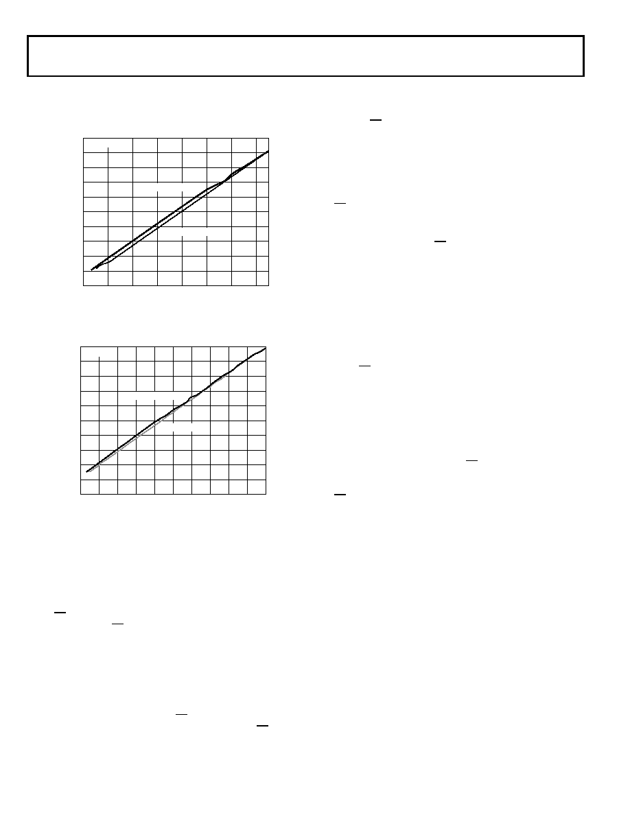
Figure 85. Power vs. Throughput in Normal Mode with VDD = 3 V
Figure 86. Power vs. Throughput in Normal Mode with VDD = 5 V
THROUGHPUT (kSPS)
1400
0
200
400
600
800
1000
1200
POWER
(mW)
10.0
9.5
9.0
8.5
8.0
7.5
7.0
6.5
6.0
5.5
5.0
24MHz ADSCLK
VARIABLE ADSCLK
TA = 25°C
THROUGHPUT (kSPS)
2000
0
200
400
600
800 1000 1200 1400 1600 1800
POWER
(mW)
30
28
26
24
22
20
18
16
14
12
10
32MHz ADSCLK
VARIABLE ADSCLK
TA = 25°C
相关PDF资料 |
PDF描述 |
|---|---|
| TPSB476K010H0500 | CAP TANT 47UF 10V 10% 1210 |
| GBC08DREN | CONN EDGECARD 16POS .100 EYELET |
| CS48540-DQZR | IC DSP HP 32BIT 8CH I/O 48-QFP |
| 2300HT-220-V-RC | INDUCTOR TOROID 22UH 15% VERT |
| JWT75-5FF/A | PS TRIPLE OUTPUT +5V/+15V/-15V |
相关代理商/技术参数 |
参数描述 |
|---|---|
| ADSP-BF506BSWZ-3F | 功能描述:IC DSP 400MHZ 1.4V 120LQFP RoHS:是 类别:集成电路 (IC) >> 嵌入式 - DSP(数字式信号处理器) 系列:Blackfin® 标准包装:40 系列:TMS320DM64x, DaVinci™ 类型:定点 接口:I²C,McASP,McBSP 时钟速率:400MHz 非易失内存:外部 芯片上RAM:160kB 电压 - 输入/输出:3.30V 电压 - 核心:1.20V 工作温度:0°C ~ 90°C 安装类型:表面贴装 封装/外壳:548-BBGA,FCBGA 供应商设备封装:548-FCBGA(27x27) 包装:托盘 配用:TMDSDMK642-0E-ND - DEVELPER KIT W/NTSC CAMERA296-23038-ND - DSP STARTER KIT FOR TMS320C6416296-23059-ND - FLASHBURN PORTING KIT296-23058-ND - EVAL MODULE FOR DM642TMDSDMK642-ND - DEVELOPER KIT W/NTSC CAMERA |
| ADSP-BF506BSWZ-4F | 功能描述:IC DSP 400MHZ 1.4V 120LQFP RoHS:是 类别:集成电路 (IC) >> 嵌入式 - DSP(数字式信号处理器) 系列:Blackfin® 标准包装:40 系列:TMS320DM64x, DaVinci™ 类型:定点 接口:I²C,McASP,McBSP 时钟速率:400MHz 非易失内存:外部 芯片上RAM:160kB 电压 - 输入/输出:3.30V 电压 - 核心:1.20V 工作温度:0°C ~ 90°C 安装类型:表面贴装 封装/外壳:548-BBGA,FCBGA 供应商设备封装:548-FCBGA(27x27) 包装:托盘 配用:TMDSDMK642-0E-ND - DEVELPER KIT W/NTSC CAMERA296-23038-ND - DSP STARTER KIT FOR TMS320C6416296-23059-ND - FLASHBURN PORTING KIT296-23058-ND - EVAL MODULE FOR DM642TMDSDMK642-ND - DEVELOPER KIT W/NTSC CAMERA |
| ADSP-BF506BSWZ-4FX | 制造商:Analog Devices 功能描述:- Trays |
| ADSP-BF506F | 制造商:Analog Devices 功能描述:LOW POWER BLACKFIN WITH ADVANCED EMBEDDED CONNECTIVITY - Bulk |
| ADSPBF506FBSWZ-ENG | 制造商:Analog Devices 功能描述:- Trays |
发布紧急采购,3分钟左右您将得到回复。