- 您现在的位置:买卖IC网 > PDF目录19403 > ADSP-BF504KCPZ-4F (Analog Devices Inc)IC CCD SIGNAL PROCESSOR 88LFCSP PDF资料下载
参数资料
| 型号: | ADSP-BF504KCPZ-4F |
| 厂商: | Analog Devices Inc |
| 文件页数: | 62/80页 |
| 文件大小: | 0K |
| 描述: | IC CCD SIGNAL PROCESSOR 88LFCSP |
| 视频文件: | Blackfin? BF50x Processor Family |
| 标准包装: | 1 |
| 系列: | Blackfin® |
| 类型: | 定点 |
| 接口: | CAN,EBI/EMI,I²C,IrDA,PPI,SPI,SPORT,UART/USART |
| 时钟速率: | 400MHz |
| 非易失内存: | 闪存(16MB) |
| 芯片上RAM: | 68kB |
| 电压 - 输入/输出: | 3.30V |
| 电压 - 核心: | 1.31V |
| 工作温度: | 0°C ~ 70°C |
| 安装类型: | 表面贴装 |
| 封装/外壳: | 88-VFQFN 裸露焊盘,CSP |
| 供应商设备封装: | 88-LFCSP(12x12) |
| 包装: | 托盘 |
第1页第2页第3页第4页第5页第6页第7页第8页第9页第10页第11页第12页第13页第14页第15页第16页第17页第18页第19页第20页第21页第22页第23页第24页第25页第26页第27页第28页第29页第30页第31页第32页第33页第34页第35页第36页第37页第38页第39页第40页第41页第42页第43页第44页第45页第46页第47页第48页第49页第50页第51页第52页第53页第54页第55页第56页第57页第58页第59页第60页第61页当前第62页第63页第64页第65页第66页第67页第68页第69页第70页第71页第72页第73页第74页第75页第76页第77页第78页第79页第80页
Rev. A
|
Page 65 of 80
|
July 2011
ADSP-BF504/ADSP-BF504F/ADSP-BF506F
to make use of the full dynamic range of the part. A dc input is
applied to the VIN– pin. The voltage applied to this input pro-
vides an offset from ground or a pseudo ground for the VIN+
input. The benefit of pseudo differential inputs is that they sepa-
rate the analog input signal ground from the ADC’s ground
allowing dc common-mode voltages to be cancelled.
The typical voltage range for the VIN– pin, while in pseudo dif-
vs. VREF in Pseudo Differential Mode with VDD = 3 V) and
Mode Connection Diagram) shows a connection diagram for
pseudo differential mode.
Analog Input Selection
The analog inputs of the ADC can be configured as single-
ended or true differential via the SGL/DIFF logic pin, as shown
tion). If this pin is tied to a logic low, the analog input channels
to each on-chip ADC are set up as three true differential pairs. If
this pin is at logic high, the analog input channels to each on-
chip ADC are set up as six single-ended analog inputs. The
required logic level on this pin needs to be established prior to
the acquisition time and remain unchanged during the conver-
sion time until the track-and-hold has returned to track. The
track-and-hold returns to track on the 13th rising edge of
ADSCLK after the CS falling edge (see Figure 87 (Serial Inter-
face Timing Diagram)). If the level on this pin is changed, it will
be recognized by the ADC; therefore, it is necessary to keep the
same logic level during acquisition and conversion to avoid cor-
rupting the conversion in progress.
For example, in Figure 77 (Selecting Differential or Single-
Ended Configuration) the SGL/DIFF pin is set at logic high for
the duration of both the acquisition and conversion times so the
analog inputs are configured as single ended for that conversion
(Sampling Point A). The logic level of the SGL/DIFF changed to
low after the track-and-hold returned to track and prior to the
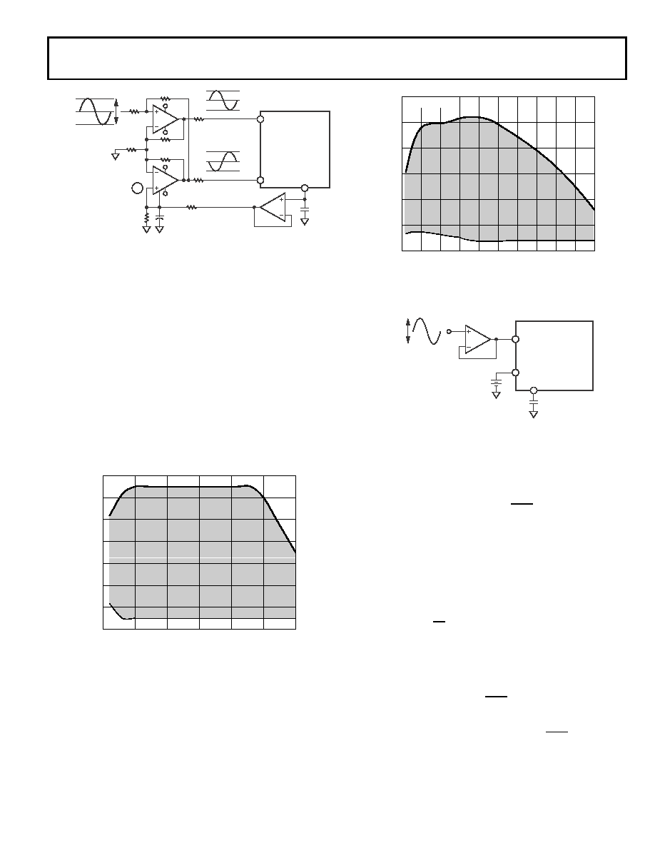
Figure 73. Dual Op Amp Circuit to Convert a Single-Ended Bipolar Signal
into a Differential Unipolar Signal
Figure 74. VIN- Input Voltage Range vs. VREF in
Pseudo Differential Mode with VDD = 3 V
20k
220k
2 × VREF p–p
27
V+
V–
V+
V–
GND
2.5V
3.75V
1.25V
2.5V
3.75V
1.25V
VIN+
ADC
1
VIN–
440
220
0.47μF
1ADDITIONAL PINS OMITTED FOR CLARITY.
220
10k
A
V
REF
(DCAPA/DCAPB)
VREF (V)
3.0
0
0.5
1.0
1.5
2.0
2.5
V
IN–
(V)
1.0
0.8
0.4
0.6
0.2
–0.2
0
–0.4
TA = 25°C
Figure 75. VIN– Input Voltage Range vs. VREF in
Pseudo Differential Mode with VDD = 5 V
Figure 76. Pseudo Differential Mode Connection Diagram
VREF (V)
5.0
0
0.5
1.0
1.5
2.0
2.5
3.0
3.5
4.0
4.5
V
IN–
(V)
2.5
2.0
1.5
1.0
0.5
0
–0.5
TA = 25°C
DC INPUT
VOLTAGE
VREF
p–p
VREF (DCAPA/DCAPB)
VIN+
ADC
1
VIN–
0.47μF
1ADDITIONAL PINS OMITTED FOR CLARITY.
相关PDF资料 |
PDF描述 |
|---|---|
| TPSB476K010H0500 | CAP TANT 47UF 10V 10% 1210 |
| GBC08DREN | CONN EDGECARD 16POS .100 EYELET |
| CS48540-DQZR | IC DSP HP 32BIT 8CH I/O 48-QFP |
| 2300HT-220-V-RC | INDUCTOR TOROID 22UH 15% VERT |
| JWT75-5FF/A | PS TRIPLE OUTPUT +5V/+15V/-15V |
相关代理商/技术参数 |
参数描述 |
|---|---|
| ADSP-BF506BSWZ-3F | 功能描述:IC DSP 400MHZ 1.4V 120LQFP RoHS:是 类别:集成电路 (IC) >> 嵌入式 - DSP(数字式信号处理器) 系列:Blackfin® 标准包装:40 系列:TMS320DM64x, DaVinci™ 类型:定点 接口:I²C,McASP,McBSP 时钟速率:400MHz 非易失内存:外部 芯片上RAM:160kB 电压 - 输入/输出:3.30V 电压 - 核心:1.20V 工作温度:0°C ~ 90°C 安装类型:表面贴装 封装/外壳:548-BBGA,FCBGA 供应商设备封装:548-FCBGA(27x27) 包装:托盘 配用:TMDSDMK642-0E-ND - DEVELPER KIT W/NTSC CAMERA296-23038-ND - DSP STARTER KIT FOR TMS320C6416296-23059-ND - FLASHBURN PORTING KIT296-23058-ND - EVAL MODULE FOR DM642TMDSDMK642-ND - DEVELOPER KIT W/NTSC CAMERA |
| ADSP-BF506BSWZ-4F | 功能描述:IC DSP 400MHZ 1.4V 120LQFP RoHS:是 类别:集成电路 (IC) >> 嵌入式 - DSP(数字式信号处理器) 系列:Blackfin® 标准包装:40 系列:TMS320DM64x, DaVinci™ 类型:定点 接口:I²C,McASP,McBSP 时钟速率:400MHz 非易失内存:外部 芯片上RAM:160kB 电压 - 输入/输出:3.30V 电压 - 核心:1.20V 工作温度:0°C ~ 90°C 安装类型:表面贴装 封装/外壳:548-BBGA,FCBGA 供应商设备封装:548-FCBGA(27x27) 包装:托盘 配用:TMDSDMK642-0E-ND - DEVELPER KIT W/NTSC CAMERA296-23038-ND - DSP STARTER KIT FOR TMS320C6416296-23059-ND - FLASHBURN PORTING KIT296-23058-ND - EVAL MODULE FOR DM642TMDSDMK642-ND - DEVELOPER KIT W/NTSC CAMERA |
| ADSP-BF506BSWZ-4FX | 制造商:Analog Devices 功能描述:- Trays |
| ADSP-BF506F | 制造商:Analog Devices 功能描述:LOW POWER BLACKFIN WITH ADVANCED EMBEDDED CONNECTIVITY - Bulk |
| ADSPBF506FBSWZ-ENG | 制造商:Analog Devices 功能描述:- Trays |
发布紧急采购,3分钟左右您将得到回复。