- 您现在的位置:买卖IC网 > PDF目录19403 > ADSP-BF504KCPZ-4F (Analog Devices Inc)IC CCD SIGNAL PROCESSOR 88LFCSP PDF资料下载
参数资料
| 型号: | ADSP-BF504KCPZ-4F |
| 厂商: | Analog Devices Inc |
| 文件页数: | 66/80页 |
| 文件大小: | 0K |
| 描述: | IC CCD SIGNAL PROCESSOR 88LFCSP |
| 视频文件: | Blackfin? BF50x Processor Family |
| 标准包装: | 1 |
| 系列: | Blackfin® |
| 类型: | 定点 |
| 接口: | CAN,EBI/EMI,I²C,IrDA,PPI,SPI,SPORT,UART/USART |
| 时钟速率: | 400MHz |
| 非易失内存: | 闪存(16MB) |
| 芯片上RAM: | 68kB |
| 电压 - 输入/输出: | 3.30V |
| 电压 - 核心: | 1.31V |
| 工作温度: | 0°C ~ 70°C |
| 安装类型: | 表面贴装 |
| 封装/外壳: | 88-VFQFN 裸露焊盘,CSP |
| 供应商设备封装: | 88-LFCSP(12x12) |
| 包装: | 托盘 |
第1页第2页第3页第4页第5页第6页第7页第8页第9页第10页第11页第12页第13页第14页第15页第16页第17页第18页第19页第20页第21页第22页第23页第24页第25页第26页第27页第28页第29页第30页第31页第32页第33页第34页第35页第36页第37页第38页第39页第40页第41页第42页第43页第44页第45页第46页第47页第48页第49页第50页第51页第52页第53页第54页第55页第56页第57页第58页第59页第60页第61页第62页第63页第64页第65页当前第66页第67页第68页第69页第70页第71页第72页第73页第74页第75页第76页第77页第78页第79页第80页
Rev. A
|
Page 69 of 80
|
July 2011
ADSP-BF504/ADSP-BF504F/ADSP-BF506F
Power-Up Times
As described in detail, the ADC has two power-down modes,
partial power-down and full power-down. This section deals
with the power-up time required when coming out of either of
these modes. It should be noted that the power-up times, as
explained in this section, apply with the recommended capaci-
tors in place on the DCAPA and DCAPB pins.
To power up from full power-down, approximately 1.5 ms
should be allowed from the falling edge of CS, shown as
ering up from partial power-down requires much less time. The
power-up time from partial power-down is typically 1 μs; how-
ever, if using the internal reference, then the ADC must be in
partial power-down for at least 67 μs in order for this power-up
time to apply.
When power supplies are first applied to the ADC, the ADC
may power up in either of the power-down modes or normal
mode. Because of this, it is best to allow a dummy cycle to elapse
to ensure the part is fully powered up before attempting a valid
conversion. Likewise, if it is intended to keep the part in the par-
tial power-down mode immediately after the supplies are
applied, then two dummy cycles must be initiated. The first
dummy cycle must hold CS low until after the 10th ADSCLK
falling edge (see Figure 80 (Normal Mode Operation)); in the
second cycle, CS must be brought high before the 10th ADSCLK
edge but after the second ADSCLK falling edge (see Figure 81
(Entering Partial Power-Down Mode)). Alternatively, if it is
intended to place the part in full power-down mode when the
supplies are applied, then three dummy cycles must be initiated.
The first dummy cycle must hold CS low until after the 10th
ADSCLK falling edge (see Figure 80 (Normal Mode Opera-
tion)); the second and third dummy cycles place the part in full
power-down (see Figure 83 (Entering Full Power-Down
Once supplies are applied to the ADC, enough time must be
allowed for any external reference to power up and charge the
various reference buffer decoupling capacitors to their final
values.
Power vs. Throughput Rate
The power consumption of the ADC varies with the throughput
rate. When using very slow throughput rates and as fast an
ADSCLK frequency as possible, the various power-down
options can be used to make significant power savings. How-
ever, the ADC quiescent current is low enough that even
without using the power-down options, there is a noticeable
variation in power consumption with sampling rate. This is true
whether a fixed ADSCLK value is used or if it is scaled with the
sampling rate. Figure 85 (Power vs. Throughput in Normal
in Normal Mode with VDD = 5 V) show plots of power vs. the
throughput rate when operating in normal mode for a fixed
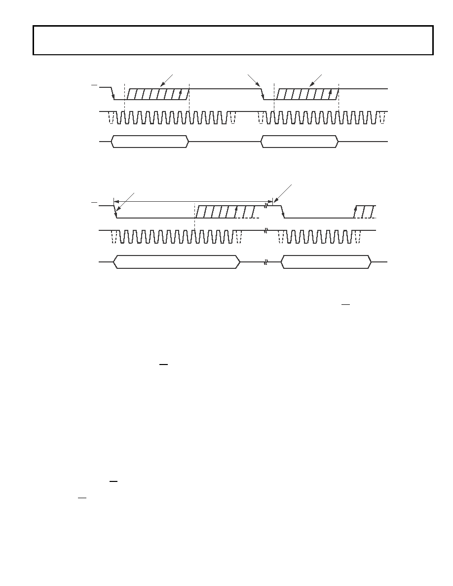
Figure 83. Entering Full Power-Down Mode
Figure 84. Exiting Full Power-Down Mode
THREE-STATE
110
14
2
ADSCLK
CS
DOUTA
DOUTB
THREE-STATE
110
14
2
INVALID DATA
THE PART BEGINS
TO POWER UP.
THE PART ENTERS
PARTIAL POWER DOWN.
THE PART ENTERS
FULL POWER DOWN.
ADSCLK
DOUTA
DOUTB
INVALID DATA
VALID DATA
1
10
14
1
THE PART BEGINS
TO POWER UP.
THE PART IS FULLY POWERED UP,
SEE POWER-UP TIMES SECTION.
tPOWER-UP2
CS
相关PDF资料 |
PDF描述 |
|---|---|
| TPSB476K010H0500 | CAP TANT 47UF 10V 10% 1210 |
| GBC08DREN | CONN EDGECARD 16POS .100 EYELET |
| CS48540-DQZR | IC DSP HP 32BIT 8CH I/O 48-QFP |
| 2300HT-220-V-RC | INDUCTOR TOROID 22UH 15% VERT |
| JWT75-5FF/A | PS TRIPLE OUTPUT +5V/+15V/-15V |
相关代理商/技术参数 |
参数描述 |
|---|---|
| ADSP-BF506BSWZ-3F | 功能描述:IC DSP 400MHZ 1.4V 120LQFP RoHS:是 类别:集成电路 (IC) >> 嵌入式 - DSP(数字式信号处理器) 系列:Blackfin® 标准包装:40 系列:TMS320DM64x, DaVinci™ 类型:定点 接口:I²C,McASP,McBSP 时钟速率:400MHz 非易失内存:外部 芯片上RAM:160kB 电压 - 输入/输出:3.30V 电压 - 核心:1.20V 工作温度:0°C ~ 90°C 安装类型:表面贴装 封装/外壳:548-BBGA,FCBGA 供应商设备封装:548-FCBGA(27x27) 包装:托盘 配用:TMDSDMK642-0E-ND - DEVELPER KIT W/NTSC CAMERA296-23038-ND - DSP STARTER KIT FOR TMS320C6416296-23059-ND - FLASHBURN PORTING KIT296-23058-ND - EVAL MODULE FOR DM642TMDSDMK642-ND - DEVELOPER KIT W/NTSC CAMERA |
| ADSP-BF506BSWZ-4F | 功能描述:IC DSP 400MHZ 1.4V 120LQFP RoHS:是 类别:集成电路 (IC) >> 嵌入式 - DSP(数字式信号处理器) 系列:Blackfin® 标准包装:40 系列:TMS320DM64x, DaVinci™ 类型:定点 接口:I²C,McASP,McBSP 时钟速率:400MHz 非易失内存:外部 芯片上RAM:160kB 电压 - 输入/输出:3.30V 电压 - 核心:1.20V 工作温度:0°C ~ 90°C 安装类型:表面贴装 封装/外壳:548-BBGA,FCBGA 供应商设备封装:548-FCBGA(27x27) 包装:托盘 配用:TMDSDMK642-0E-ND - DEVELPER KIT W/NTSC CAMERA296-23038-ND - DSP STARTER KIT FOR TMS320C6416296-23059-ND - FLASHBURN PORTING KIT296-23058-ND - EVAL MODULE FOR DM642TMDSDMK642-ND - DEVELOPER KIT W/NTSC CAMERA |
| ADSP-BF506BSWZ-4FX | 制造商:Analog Devices 功能描述:- Trays |
| ADSP-BF506F | 制造商:Analog Devices 功能描述:LOW POWER BLACKFIN WITH ADVANCED EMBEDDED CONNECTIVITY - Bulk |
| ADSPBF506FBSWZ-ENG | 制造商:Analog Devices 功能描述:- Trays |
发布紧急采购,3分钟左右您将得到回复。