- 您现在的位置:买卖IC网 > PDF目录11791 > ADUC7129BSTZ126-RL (Analog Devices Inc)IC DAS MCU ARM7 ADC/DDS 80-LQFP PDF资料下载
参数资料
| 型号: | ADUC7129BSTZ126-RL |
| 厂商: | Analog Devices Inc |
| 文件页数: | 27/92页 |
| 文件大小: | 0K |
| 描述: | IC DAS MCU ARM7 ADC/DDS 80-LQFP |
| 产品培训模块: | ARM7 Applications & Tools Intro to ARM7 Core & Microconverters Process Control Direct Digital Synthesis Tutorial Series (1 of 7): Introduction |
| 标准包装: | 1 |
| 系列: | MicroConverter® ADuC7xxx |
| 核心处理器: | ARM7 |
| 芯体尺寸: | 16/32-位 |
| 速度: | 41.78MHz |
| 连通性: | EBI/EMI,I²C,SPI,UART/USART |
| 外围设备: | PLA,POR,PWM,PSM,温度传感器,WDT |
| 输入/输出数: | 38 |
| 程序存储器容量: | 126KB(63K x 16) |
| 程序存储器类型: | 闪存 |
| RAM 容量: | 8K x 8 |
| 电压 - 电源 (Vcc/Vdd): | 3 V ~ 3.6 V |
| 数据转换器: | A/D 10x12b; D/A 1x10b |
| 振荡器型: | 内部 |
| 工作温度: | -40°C ~ 125°C |
| 封装/外壳: | 80-LQFP |
| 包装: | 标准包装 |
| 其它名称: | ADUC7129BSTZ126-RLDKR |
第1页第2页第3页第4页第5页第6页第7页第8页第9页第10页第11页第12页第13页第14页第15页第16页第17页第18页第19页第20页第21页第22页第23页第24页第25页第26页当前第27页第28页第29页第30页第31页第32页第33页第34页第35页第36页第37页第38页第39页第40页第41页第42页第43页第44页第45页第46页第47页第48页第49页第50页第51页第52页第53页第54页第55页第56页第57页第58页第59页第60页第61页第62页第63页第64页第65页第66页第67页第68页第69页第70页第71页第72页第73页第74页第75页第76页第77页第78页第79页第80页第81页第82页第83页第84页第85页第86页第87页第88页第89页第90页第91页第92页
ADuC7128/ADuC7129
Rev. 0 | Page 33 of 92
O
U
T
P
UT
CO
DE
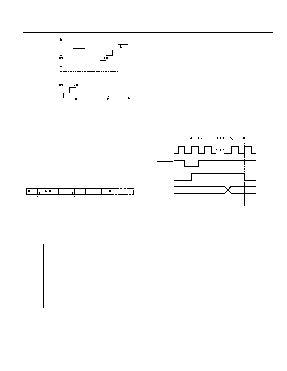
VOLTAGE INPUT (VIN+–VIN–)
0 1111 1111 1110
0 1111 1111 1100
0 1111 1111 1010
0 0000 0000 0001
0 0000 0000 0000
1 1111 1111 1110
1 0000 0000 0100
1 0000 0000 0010
1 0000 0000 0000
–VREF +1LSB
+VREF –1LSB
0LSB
1LSB =
2× VREF
4096
SIGN
BIT
06
02
0-
0
30
Current Consumption
The ADC in standby mode, that is, powered up but not
converting, typically consumes 640 μA. The internal reference
adds 140 μA. During conversion, the extra current is 0.3 μA,
multiplied by the sampling frequency (in kHz).
Timing
Figure 36 gives details of the ADC timing. Users control the
ADC clock speed and the number of acquisition clock in the
ADCCON MMR. By default, the acquisition time is eight clocks
and the clock divider is two. The number of extra clocks (such
as bit trial or write) is set to 19, giving a sampling rate of 774 kSPS.
For conversion on the temperature sensor, the ADC acquisition
time is automatically set to 16 clocks and the ADC clock divider
is set to 32. When using multiple channels, including the
temperature sensor, the timing settings revert back to the user-
defined settings after reading the temperature sensor channel.
Figure 34. ADC Transfer Function in Differential Mode
TYPICAL OPERATION
Once configured via the ADC control and channel selection
registers, the ADC converts the analog input and provides
an 11-bit result in the ADC data register.
ADC CLOCK
ACQ
BIT TRIAL
DATA
ADCSTA = 0
ADCSTA = 1
ADC INTERRUPT
WRITE
CONVSTART
ADCBUSY
ADCDAT
06
020-
032
The top four bits are the sign bits, and the 12-bit result is placed
from Bit 16 to Bit 27, as shown in Figure 35. For fully differential
mode, the result is ±11 bits. Again, it should be noted that in
fully differential mode, the result is represented in twos comple-
ment format shifted one bit to the right, and in pseudo differential
and single-ended mode, the result is represented in straight
binary format.
SIGN BITS
12-BIT ADC RESULT
3127
16 15
0
06
02
0
-03
1
Figure 35. ADC Result Format
Figure 36. ADC Timing
ADC MMRs Interface
The ADC is controlled and configured via a number of MMRs (see Table 32) that are described in detail in the following pages.
Table 32. ADC MMRs
Name
Description
ADCCON
ADC Control Register. Allows the programmer to enable the ADC peripheral, to select the mode of operation of the ADC (either
single-ended, pseudo differential, or fully differential mode), and to select the conversion type (see Table 33).
ADCCP
ADC Positive Channel Selection Register.
ADCCN
ADC Negative Channel Selection Register.
ADCSTA
ADC Status Register. Indicates when an ADC conversion result is ready. The ADCSTA register contains only one bit, ADCREADY
(Bit 0), representing the status of the ADC. This bit is set at the end of an ADC conversion generating an ADC interrupt. It is
cleared automatically by reading the ADCDAT MMR. When the ADC is performing a conversion, the status of the ADC can be
read externally via the ADCBusy pin. This pin is high during a conversion. When the conversion is finished, ADCBusy goes back low.
This information can be available on P0.5 (see the General-Purpose I/O section) if enabled in the GP0CON register.
ADCDAT
ADC Data Result Register. Holds the 12-bit ADC result, as shown in Table 35.
ADCRST
ADC Reset Register. Resets all the ADC registers to their default values.
相关PDF资料 |
PDF描述 |
|---|---|
| D38999/20FC8SC | CONN RCPT 8POS WALL MNT W/SCKT |
| D38999/26WC8PB | CONN PLUG 8POS STRAIGHT W/PINS |
| MS27473E18A11P | CONN PLUG 11POS STRAIGHT W/PINS |
| AT32UC3C2512C-Z2ZR | IC MCU AVR32 512K FLASH 64QFN |
| MS27484E10B98P | CONN PLUG 6POS STRAIGHT W/PINS |
相关代理商/技术参数 |
参数描述 |
|---|---|
| ADUC7129BSTZ126-RL2 | 制造商:AD 制造商全称:Analog Devices 功能描述:Precision Analog Microcontroller ARM7TDMI MCU with 12-Bit ADC and DDS DAC |
| aduc7229bcpz126 | 制造商:Analog Devices 功能描述: |
| ADUC7229BCPZ126-RL | 制造商:Analog Devices 功能描述: |
| ADUC812 | 制造商:AD 制造商全称:Analog Devices 功能描述:MicroConverter⑩, Multichannel 12-Bit ADC with Embedded FLASH MCU |
| ADUC812_03 | 制造商:AD 制造商全称:Analog Devices 功能描述:MicroConverter㈢, Multichannel 12-Bit ADC with Embedded Flash MCU |
发布紧急采购,3分钟左右您将得到回复。