- 您现在的位置:买卖IC网 > PDF目录11791 > ADUC7129BSTZ126-RL (Analog Devices Inc)IC DAS MCU ARM7 ADC/DDS 80-LQFP PDF资料下载
参数资料
| 型号: | ADUC7129BSTZ126-RL |
| 厂商: | Analog Devices Inc |
| 文件页数: | 30/92页 |
| 文件大小: | 0K |
| 描述: | IC DAS MCU ARM7 ADC/DDS 80-LQFP |
| 产品培训模块: | ARM7 Applications & Tools Intro to ARM7 Core & Microconverters Process Control Direct Digital Synthesis Tutorial Series (1 of 7): Introduction |
| 标准包装: | 1 |
| 系列: | MicroConverter® ADuC7xxx |
| 核心处理器: | ARM7 |
| 芯体尺寸: | 16/32-位 |
| 速度: | 41.78MHz |
| 连通性: | EBI/EMI,I²C,SPI,UART/USART |
| 外围设备: | PLA,POR,PWM,PSM,温度传感器,WDT |
| 输入/输出数: | 38 |
| 程序存储器容量: | 126KB(63K x 16) |
| 程序存储器类型: | 闪存 |
| RAM 容量: | 8K x 8 |
| 电压 - 电源 (Vcc/Vdd): | 3 V ~ 3.6 V |
| 数据转换器: | A/D 10x12b; D/A 1x10b |
| 振荡器型: | 内部 |
| 工作温度: | -40°C ~ 125°C |
| 封装/外壳: | 80-LQFP |
| 包装: | 标准包装 |
| 其它名称: | ADUC7129BSTZ126-RLDKR |
第1页第2页第3页第4页第5页第6页第7页第8页第9页第10页第11页第12页第13页第14页第15页第16页第17页第18页第19页第20页第21页第22页第23页第24页第25页第26页第27页第28页第29页当前第30页第31页第32页第33页第34页第35页第36页第37页第38页第39页第40页第41页第42页第43页第44页第45页第46页第47页第48页第49页第50页第51页第52页第53页第54页第55页第56页第57页第58页第59页第60页第61页第62页第63页第64页第65页第66页第67页第68页第69页第70页第71页第72页第73页第74页第75页第76页第77页第78页第79页第80页第81页第82页第83页第84页第85页第86页第87页第88页第89页第90页第91页第92页
ADuC7128/ADuC7129
Rev. 0 | Page 36 of 92
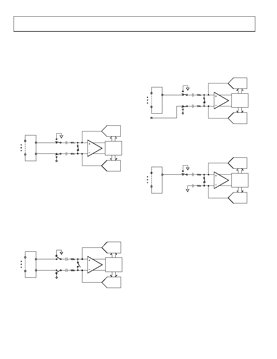
CONVERTER OPERATION
The ADC incorporates a successive approximation (SAR)
architecture involving a charge-sampled input stage. This
architecture is described for the three different modes of
operation: differential mode, pseudo differential mode, and
single-ended mode.
Differential Mode
The ADuC7128/ADuC7129 contain a successive approximation
show simplified schematics of the ADC in acquisition and
conversion phase, respectively. The ADC comprises control logic,
a SAR, and two capacitive DACs. In Figure 37 (the acquisition
phase), SW3 is closed and SW1 and SW2 are in Position A. The
comparator is held in a balanced condition, and the sampling
capacitor arrays acquire the differential signal on the input.
CAPACITIVE
DAC
CAPACITIVE
DAC
CONTROL
LOGIC
COMPARATOR
SW3
SW1
A
B
SW2
CS
VREF
AIN0
AIN13
MUX
CHANNEL+
CHANNEL–
06020-
033
Figure 37. ADC Acquisition Phase
When the ADC starts a conversion (see Figure 38), SW3 opens
and SW1 and SW2 move to Position B, causing the comparator
to become unbalanced. Both inputs are disconnected once the
conversion begins. The control logic and the charge redistribution
DACs are used to add and subtract fixed amounts of charge
from the sampling capacitor arrays to bring the comparator
back into a balanced condition. When the comparator is
rebalanced, the conversion is complete. The control logic generates
the ADC output code. The output impedances of the sources
driving the VIN+ pin and the VIN pin must be matched; otherwise,
the two inputs have different settling times, resulting in errors.
CAPACITIVE
DAC
CAPACITIVE
DAC
CONTROL
LOGIC
COMPARATOR
SW3
SW1
A
B
SW2
CS
VREF
AIN0
AIN13
MUX
CHANNEL+
CHANNEL–
0602
0-
03
4
Figure 38. ADC Conversion Phase
Pseudo Differential Mode
In pseudo differential mode, Channel is linked to the VIN pin
of the ADuC7128/ADuC7129, and SW2 switches between A
(Channel) and B (VREF). The VIN pin must be connected to
ground or a low voltage. The input signal on VIN+ can then vary
from VIN to VREF + VIN. Note that VIN must be chosen so that
VREF + VIN does not exceed AVDD.
CAPACITIVE
DAC
CAPACITIVE
DAC
CONTROL
LOGIC
COMPARATOR
SW3
SW1
A
B
SW2
CS
VREF
AIN0
AIN13
VIN–
MUX
CHANNEL+
CHANNEL–
0602
0-
03
5
Figure 39. ADC in Pseudo Differential Mode
Single-Ended Mode
In single-ended mode, SW2 is always connected internally to
ground. The VIN pin can be floating. The input signal range on
VIN+ is 0 V to VREF.
CAPACITIVE
DAC
CAPACITIVE
DAC
CONTROL
LOGIC
COMPARATOR
SW3
SW1
A
B
CS
AIN0
AIN13
MUX
CHANNEL+
CHANNEL–
0602
0-
03
6
Figure 40. ADC in Single-Ended Mode
Analog Input Structure
Figure 41 shows the equivalent circuit of the analog input
structure of the ADC. The four diodes provide ESD protection
for the analog inputs. Care must be taken to ensure that the
analog input signals never exceed the supply rails by more than
300 mV. Voltage in excess of 300 mV would cause these diodes to
become forward biased and start conducting into the substrate.
These diodes can conduct up to 10 mA without causing
irreversible damage to the part.
The C1 capacitors in Figure 41 are typically 4 pF and can be
primarily attributed to pin capacitance. The resistors are lumped
components made up of the on resistance of the switches. The
value of these resistors is typically about 100 Ω. The C2 capacitors
are the ADC sampling capacitors and have a capacitance of 16 pF
typical.
相关PDF资料 |
PDF描述 |
|---|---|
| D38999/20FC8SC | CONN RCPT 8POS WALL MNT W/SCKT |
| D38999/26WC8PB | CONN PLUG 8POS STRAIGHT W/PINS |
| MS27473E18A11P | CONN PLUG 11POS STRAIGHT W/PINS |
| AT32UC3C2512C-Z2ZR | IC MCU AVR32 512K FLASH 64QFN |
| MS27484E10B98P | CONN PLUG 6POS STRAIGHT W/PINS |
相关代理商/技术参数 |
参数描述 |
|---|---|
| ADUC7129BSTZ126-RL2 | 制造商:AD 制造商全称:Analog Devices 功能描述:Precision Analog Microcontroller ARM7TDMI MCU with 12-Bit ADC and DDS DAC |
| aduc7229bcpz126 | 制造商:Analog Devices 功能描述: |
| ADUC7229BCPZ126-RL | 制造商:Analog Devices 功能描述: |
| ADUC812 | 制造商:AD 制造商全称:Analog Devices 功能描述:MicroConverter⑩, Multichannel 12-Bit ADC with Embedded FLASH MCU |
| ADUC812_03 | 制造商:AD 制造商全称:Analog Devices 功能描述:MicroConverter㈢, Multichannel 12-Bit ADC with Embedded Flash MCU |
发布紧急采购,3分钟左右您将得到回复。