- 您现在的位置:买卖IC网 > PDF目录11791 > ADUC7129BSTZ126-RL (Analog Devices Inc)IC DAS MCU ARM7 ADC/DDS 80-LQFP PDF资料下载
参数资料
| 型号: | ADUC7129BSTZ126-RL |
| 厂商: | Analog Devices Inc |
| 文件页数: | 86/92页 |
| 文件大小: | 0K |
| 描述: | IC DAS MCU ARM7 ADC/DDS 80-LQFP |
| 产品培训模块: | ARM7 Applications & Tools Intro to ARM7 Core & Microconverters Process Control Direct Digital Synthesis Tutorial Series (1 of 7): Introduction |
| 标准包装: | 1 |
| 系列: | MicroConverter® ADuC7xxx |
| 核心处理器: | ARM7 |
| 芯体尺寸: | 16/32-位 |
| 速度: | 41.78MHz |
| 连通性: | EBI/EMI,I²C,SPI,UART/USART |
| 外围设备: | PLA,POR,PWM,PSM,温度传感器,WDT |
| 输入/输出数: | 38 |
| 程序存储器容量: | 126KB(63K x 16) |
| 程序存储器类型: | 闪存 |
| RAM 容量: | 8K x 8 |
| 电压 - 电源 (Vcc/Vdd): | 3 V ~ 3.6 V |
| 数据转换器: | A/D 10x12b; D/A 1x10b |
| 振荡器型: | 内部 |
| 工作温度: | -40°C ~ 125°C |
| 封装/外壳: | 80-LQFP |
| 包装: | 标准包装 |
| 其它名称: | ADUC7129BSTZ126-RLDKR |
第1页第2页第3页第4页第5页第6页第7页第8页第9页第10页第11页第12页第13页第14页第15页第16页第17页第18页第19页第20页第21页第22页第23页第24页第25页第26页第27页第28页第29页第30页第31页第32页第33页第34页第35页第36页第37页第38页第39页第40页第41页第42页第43页第44页第45页第46页第47页第48页第49页第50页第51页第52页第53页第54页第55页第56页第57页第58页第59页第60页第61页第62页第63页第64页第65页第66页第67页第68页第69页第70页第71页第72页第73页第74页第75页第76页第77页第78页第79页第80页第81页第82页第83页第84页第85页当前第86页第87页第88页第89页第90页第91页第92页
ADuC7128/ADuC7129
Rev. 0 | Page 87 of 92
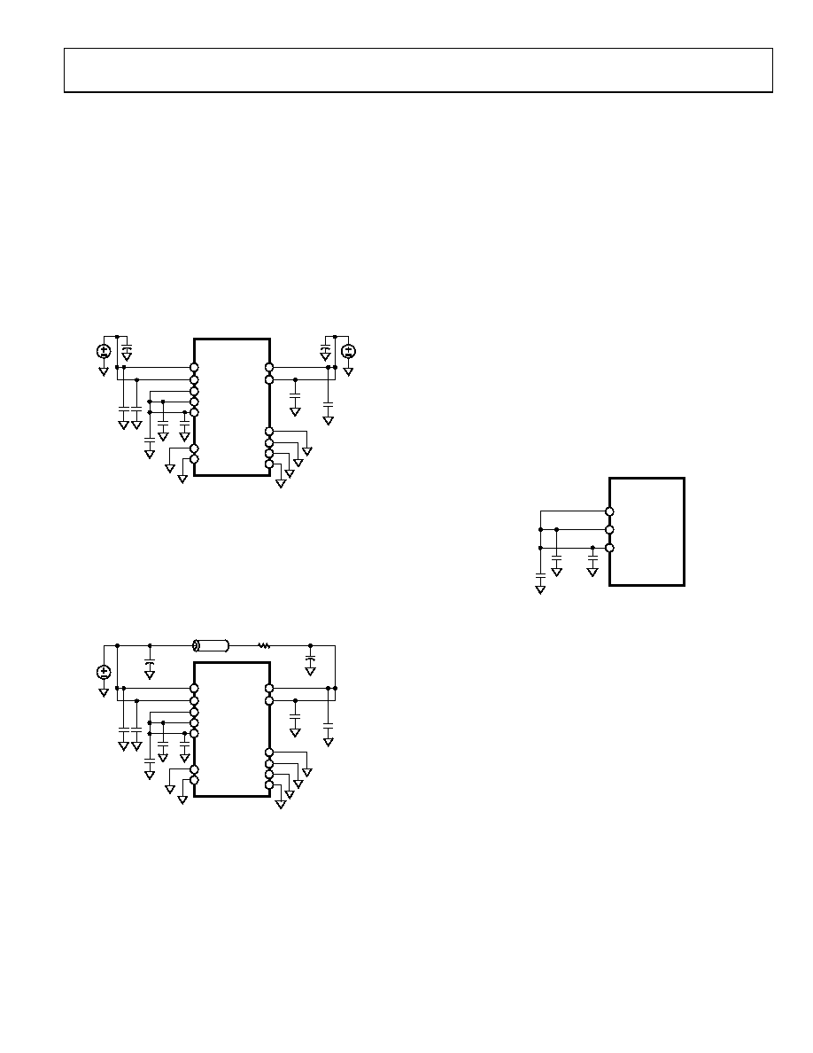
HARDWARE DESIGN CONSIDERATIONS
POWER SUPPLIES
The ADuC7128/ADuC7129 operational power supply voltage
range is 3.0 V to 3.6 V. Separate analog and digital power supply
pins (AVDD and IOVDD, respectively) allow AVDD to be kept
relatively free of noisy digital signals often present on the system
IOVDD line. In this mode, the part can also operate with split
supplies, that is, using different voltage supply levels for each
supply. For example, the system can be designed to operate with
an IOVDD voltage level of 3.3 V while the AVDD level can be at
3 V, or vice versa, if required. A typical split supply configuration
is shown in Figure 66.
+
ANALOG SUPPLY
+
DIGITAL SUPPLY
AVDD
GNDREF
DACGND
AGND
REFGND
IOVDD
LVDD
PVDD
DACVDD
IOGND
ADuC7128
10F
0.
1
F
0.1F
0.47F
0.1F
0
60
20
-05
6
Figure 66. External Dual Supply Connections
As an alternative to providing two separate power supplies, the
user can help keep AVDD quiet by placing a small series resistor
and/or ferrite bead between AVDD and IOVDD, and then decoupling
AVDD separately to ground. An example of this configuration is
shown in Figure 67. With this configuration, other analog circuitry
(such as op amps or voltage references) can be powered from
the AVDD supply line as well.
+
DIGITAL SUPPLY
AVDD
GNDREF
DACGND
AGND
REFGND
IOVDD
LVDD
PVDD
DACVDD
IOGND
ADuC7128
10F
0.
1
F
0.1F
0.47F
0.1F
BEAD
1.6V
06
02
0-
05
7
Figure 67. External Single Supply Connections
Note that in both Figure 66 and Figure 67, a large value (10 μF)
reservoir capacitor sits on IOVDD and a separate 10 μF capacitor
sits on AVDD. In addition, local small value (0.1 μF) capacitors
are located at each AVDD and IOVDD pin of the chip. As per
standard design practice, be sure to include all of these capaci-
tors and ensure that the smaller capacitors are close to each
AVDD pin with trace lengths as short as possible.
Connect the ground terminal of each of these capacitors directly
to the underlying ground plane. It should also be noted that, at
all times, the analog and digital ground pins on the ADuC7128/
ADuC7129 must be referenced to the same system ground refer-
ence point.
Finally, on the LFCSP package, the paddle on the bottom of the
package should be soldered to a metal plate to provide mechanical
stability. The metal plate should be connected to ground.
Linear Voltage Regulator
The ADuC7128/ADuC7129 require a single 3.3 V supply, but
the core logic requires a 2.5 V supply. An on-chip linear regulator
generates the 2.5 V from IOVDD for the core logic. The LVDD pin
is the 2.5 V supply for the core logic. The DAC logic and PLL logic
also require a 2.5 V supply that must be connected externally from
the LVDD pin to the DACVDD pin and the PVDD pin. An external
compensation capacitor of 0.47 μF must be connected between
LVDD and DGND (as close as possible to these pins) to act as a
tank of charge, as shown in Figure 68. In addition, decoupling
capacitors of 0.1 μF must be placed as close as possible to the
PVDD pin and the DACVDD pin.
LVDD
PVDD
DACVDD
ADuC7128
0.1F
0.47F
06
02
0-
05
8
Figure 68. Voltage Regulator Connections
The LVDD pin should not be used for any other chip. It is also
recommended that the IOVDD have excellent power supply
decoupling to help improve line regulation performance of the
on-chip voltage regulator.
GROUNDING AND BOARD LAYOUT
RECOMMENDATIONS
As with all high resolution data converters, special attention
must be paid to grounding and PC board layout of the design to
achieve optimum performance from the ADCs and DAC.
Although the ADuC7128/ADuC7129 have separate pins for
analog and digital ground (AGND and IOGND), the user must
not tie these to two separate ground planes unless the two ground
planes are connected together very close to the ADuC7128/
ADuC7129, as illustrated in the simplified example of Figure 69a.
In systems where digital and analog ground planes are connected
together somewhere else (for example, at the system power
supply), they cannot be connected again near the ADuC7128/
ADuC7129 because a ground loop results.
相关PDF资料 |
PDF描述 |
|---|---|
| D38999/20FC8SC | CONN RCPT 8POS WALL MNT W/SCKT |
| D38999/26WC8PB | CONN PLUG 8POS STRAIGHT W/PINS |
| MS27473E18A11P | CONN PLUG 11POS STRAIGHT W/PINS |
| AT32UC3C2512C-Z2ZR | IC MCU AVR32 512K FLASH 64QFN |
| MS27484E10B98P | CONN PLUG 6POS STRAIGHT W/PINS |
相关代理商/技术参数 |
参数描述 |
|---|---|
| ADUC7129BSTZ126-RL2 | 制造商:AD 制造商全称:Analog Devices 功能描述:Precision Analog Microcontroller ARM7TDMI MCU with 12-Bit ADC and DDS DAC |
| aduc7229bcpz126 | 制造商:Analog Devices 功能描述: |
| ADUC7229BCPZ126-RL | 制造商:Analog Devices 功能描述: |
| ADUC812 | 制造商:AD 制造商全称:Analog Devices 功能描述:MicroConverter⑩, Multichannel 12-Bit ADC with Embedded FLASH MCU |
| ADUC812_03 | 制造商:AD 制造商全称:Analog Devices 功能描述:MicroConverter㈢, Multichannel 12-Bit ADC with Embedded Flash MCU |
发布紧急采购,3分钟左右您将得到回复。