参数资料
| 型号: | AFE7222IRGCT |
| 厂商: | Texas Instruments |
| 文件页数: | 100/106页 |
| 文件大小: | 0K |
| 描述: | IC AFE 12BIT 65/130MSPS 64VQFN |
| 标准包装: | 1 |
| 位数: | 12 |
| 通道数: | 4 |
| 功率(瓦特): | 610mW |
| 电压 - 电源,模拟: | 2.85 V ~ 3.6 V |
| 电压 - 电源,数字: | 1.7 V ~ 1.9 V |
| 封装/外壳: | 64-VFQFN 裸露焊盘 |
| 供应商设备封装: | 64-VQFN 裸露焊盘(9x9) |
| 包装: | 标准包装 |
| 其它名称: | 296-30113-6 |
第1页第2页第3页第4页第5页第6页第7页第8页第9页第10页第11页第12页第13页第14页第15页第16页第17页第18页第19页第20页第21页第22页第23页第24页第25页第26页第27页第28页第29页第30页第31页第32页第33页第34页第35页第36页第37页第38页第39页第40页第41页第42页第43页第44页第45页第46页第47页第48页第49页第50页第51页第52页第53页第54页第55页第56页第57页第58页第59页第60页第61页第62页第63页第64页第65页第66页第67页第68页第69页第70页第71页第72页第73页第74页第75页第76页第77页第78页第79页第80页第81页第82页第83页第84页第85页第86页第87页第88页第89页第90页第91页第92页第93页第94页第95页第96页第97页第98页第99页当前第100页第101页第102页第103页第104页第105页第106页
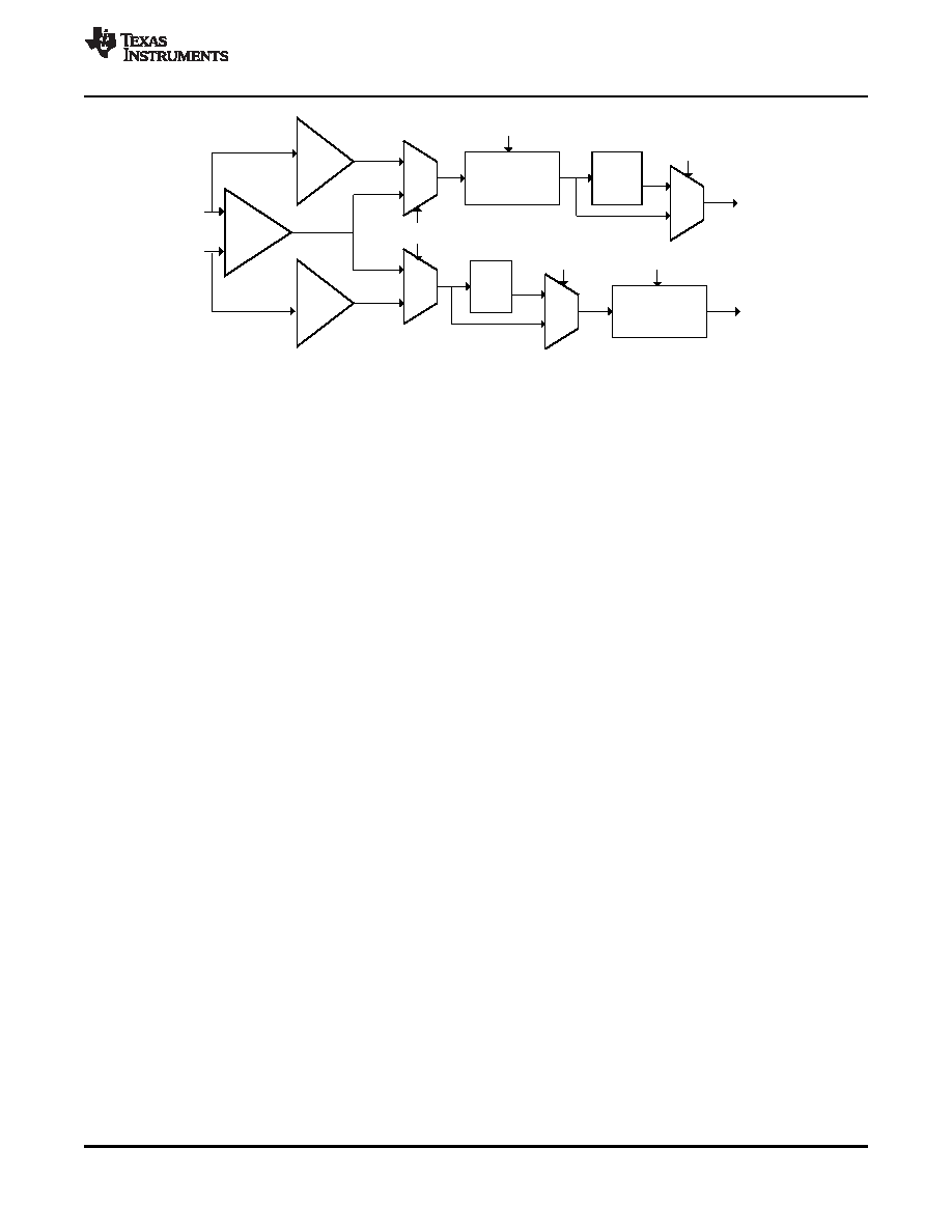
CLKINP
CLKINN
Clock
Divider
%1,2,4
Clock
Divider
%1,2,4
PLL
X2,4
ADC_CLK
DAC_CLK
MUX
PLL_ENABLE
REG_SE_CLK
DIV_ADC<1:0>
DIV_DAC<1:0>
DCC
(Duty Cycle
Correction)
MUX
ENABLE_DCC
Single-
ended
Buffer
Single-
ended
Buffer
Differential
Buffer
SLOS711B – NOVEMBER 2011 – REVISED MARCH 2012
Figure 10-20. Block Diagram of Clocking Path
Three cases are considered:
Case 1: DAC_CLK and ADC_CLK are at same rate: In this case, either CLKINP and CLKINN should be
driven by a differential clock (common to both the ADC and DAC) or two single ended clocks, both at the
same rate.
Case 2: DAC_CLK and ADC_CLK are at different rates such that the higher rate is 2X or 4X of the
lower rate: In this case, we again recommend driving CLKINP/CLKINN differentially (or by two equal rate
single ended clocks) at the higher of two rates and dividng internally by the factor of 2 (or 4) on the
channel that requires the lower rate clock.
Case 3: DAC_CLK and ADC_CLK are at different rates with the DAC_CLK being at 8X or 16X of the
ADC_CLK: In this case, we recommend driving CLKINP/CLKINN differentially (or by two equal rate single
ended clocks) at 4X of ADC_CLK rate, dividing it by 4 for the ADC, and multiplying it by 2 (or 4) for the
DAC.
Case 4: DAC_CLK and ADC_CLK are at different rates that are harmonically related but not at rates
covered by Case 2 or Case 3: In this case, there is no alternative but to drive CLKINP and CLKINN with
two different rate clocks. If phase control of the two clocks is possible, we recommend that the phases be
adjusted such that the two clocks have rise/fall edges that do not come within 5 ns of each other. We also
recommend that the driving clock rates be as close to each other as possible.
Case 5: DAC_CLK and ADC_CLK are at different rates that are non-harmonically related: This is the
worst case and it is recommended to avoid operating the AFE in full duplex mode with such clock rates.
The presence of non-harmonically related clocks at two adjacent pins can cause periodic modulation in
the sampling instant that can result in huge spurs that get worse at higher ADC input frequencies (and
DAC output frequencies). At 70 MHz IF, these spur levels could be as large as –45 dBc.
10.12 Half Duplex Operation – Coupling Considerations
If the ADC and DAC are driven externally by unequal rate clocks, then ensure that these clocks are not on
simultaneously. For example, in half duplex mode with the Tx active, ensure that the ADC clock to the
device is shut off. If the ADC and DAC are driven by equal rate clocks, then it is not required to shut off
the ADC clock when the Tx is active (and DAC clock when the Rx is active).
10.13 Half Duplex Operation Through a Common I/O Interface
If the AFE7222/7225 is to be always operated in Half Duplex mode through a common I/O interface for the
RX and TX (to reuse the same bus), then the RX and TX data and clocks can be tied on the board as
illustrated below:
Copyright 2011–2012, Texas Instruments Incorporated
DIGITAL INTERFACE
93
相关PDF资料 |
PDF描述 |
|---|---|
| ALD2502PBL | IC TIMER CMOS DUAL HS 14PDIP |
| ALD4501PEL | IC TIMER PREC CMOS QUAD 20PDIP |
| ALD500AUSWCL | IC ADC 18BIT DUAL 16WSOIC |
| ALD500RAU-10SEL | IC ADC 18BIT 20SOIC |
| ALD555PAL | IC TIMER PREC CMOS SGL HS 8PDIP |
相关代理商/技术参数 |
参数描述 |
|---|---|
| AFE7225 | 制造商:TI 制造商全称:Texas Instruments 功能描述:Analog Front End Wideband Mixed-Signal Transceiver |
| AFE7225EVM | 功能描述:射频开发工具 AFE7225 Eval Mod RoHS:否 制造商:Taiyo Yuden 产品:Wireless Modules 类型:Wireless Audio 工具用于评估:WYSAAVDX7 频率: 工作电源电压:3.4 V to 5.5 V |
| AFE7225IRGC25 | 功能描述:射频前端 Dual 12B,125MSPS ADC RoHS:否 制造商:Skyworks Solutions, Inc. 类型: 工作频率:2.4 GHz, 5 GHz 最大数据速率:54 Mbps 噪声系数: 工作电源电压:3.3 V 电源电流:180 mA 最大工作温度:+ 85 C 安装风格:SMD/SMT 封装 / 箱体:QFN-32 |
| AFE7225IRGCR | 功能描述:射频前端 Dual 12B,125MSPS ADC RoHS:否 制造商:Skyworks Solutions, Inc. 类型: 工作频率:2.4 GHz, 5 GHz 最大数据速率:54 Mbps 噪声系数: 工作电源电压:3.3 V 电源电流:180 mA 最大工作温度:+ 85 C 安装风格:SMD/SMT 封装 / 箱体:QFN-32 |
| AFE7225IRGCT | 功能描述:射频前端 Dual 12B,125MSPS ADC RoHS:否 制造商:Skyworks Solutions, Inc. 类型: 工作频率:2.4 GHz, 5 GHz 最大数据速率:54 Mbps 噪声系数: 工作电源电压:3.3 V 电源电流:180 mA 最大工作温度:+ 85 C 安装风格:SMD/SMT 封装 / 箱体:QFN-32 |
发布紧急采购,3分钟左右您将得到回复。