参数资料
| 型号: | AFE7222IRGCT |
| 厂商: | Texas Instruments |
| 文件页数: | 15/106页 |
| 文件大小: | 0K |
| 描述: | IC AFE 12BIT 65/130MSPS 64VQFN |
| 标准包装: | 1 |
| 位数: | 12 |
| 通道数: | 4 |
| 功率(瓦特): | 610mW |
| 电压 - 电源,模拟: | 2.85 V ~ 3.6 V |
| 电压 - 电源,数字: | 1.7 V ~ 1.9 V |
| 封装/外壳: | 64-VFQFN 裸露焊盘 |
| 供应商设备封装: | 64-VQFN 裸露焊盘(9x9) |
| 包装: | 标准包装 |
| 其它名称: | 296-30113-6 |
第1页第2页第3页第4页第5页第6页第7页第8页第9页第10页第11页第12页第13页第14页当前第15页第16页第17页第18页第19页第20页第21页第22页第23页第24页第25页第26页第27页第28页第29页第30页第31页第32页第33页第34页第35页第36页第37页第38页第39页第40页第41页第42页第43页第44页第45页第46页第47页第48页第49页第50页第51页第52页第53页第54页第55页第56页第57页第58页第59页第60页第61页第62页第63页第64页第65页第66页第67页第68页第69页第70页第71页第72页第73页第74页第75页第76页第77页第78页第79页第80页第81页第82页第83页第84页第85页第86页第87页第88页第89页第90页第91页第92页第93页第94页第95页第96页第97页第98页第99页第100页第101页第102页第103页第104页第105页第106页
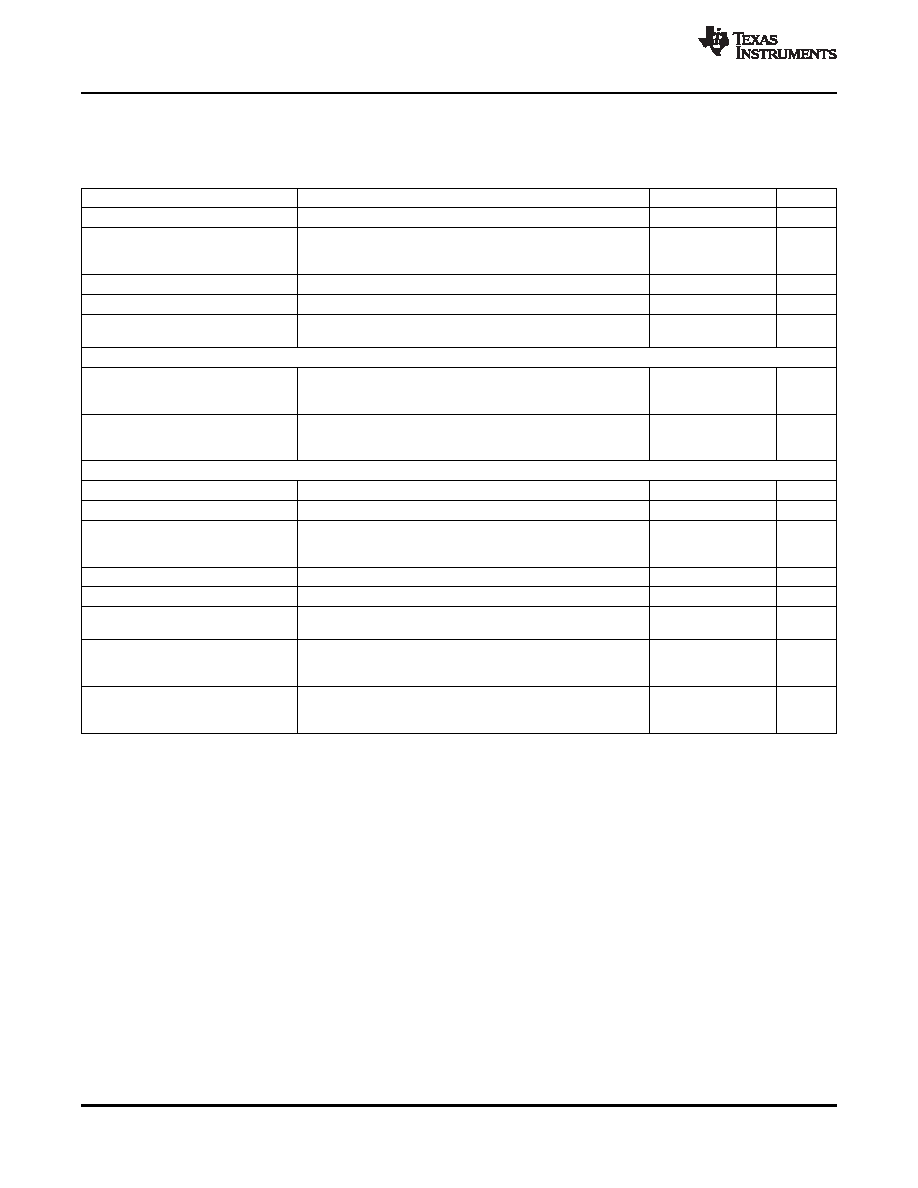
SLOS711B – NOVEMBER 2011 – REVISED MARCH 2012
Typical values are at 25°C, AVDD3_DAC = 3.0 V, AVDD3_AUX = 3.0 V, AVDD18_ADC = 1.8 V, DVDD18_CLK = 1.8 V,
DVDD18_DAC = 1.8 V, DVDD18 = 1.8 V, sampling frequency = 125 MSPS, sine wave input clock, 1.5 Vpp clock amplitude,
CLOAD = 5 pF
(1), R
LOAD = 100 Ω
(2), unless otherwise noted. Min and max values are across the full temperature range T
MIN = -
40°C to TMAX = 85°C, AVDD3_DAC = 3.0 V, AVDD3_AUX = 3.0 V, AVDD18_ADC = 1.8 V, DVDD18_CLK = 1.8 V,
DVDD18_DAC = 1.8 V, DVDD18 = 1.7 V to 1.9 V
PARAMETER
TEST CONDITIONS
MIN
TYP MAX
UNIT
th
Data hold time (5)
Zero-crossing of CLKOUTP to data becoming invalid (5)
0.26
0.4
ns
Input clock rising edge cross-over to output clock rising edge
tPDI
Clock propagation delay
cross-over 10 MSPS
≤ Sampling frequency ≤ 65 MSPS Ts =
tPDI = 0.5*Ts + tDELAY
ns
1/Sampling frequency
tdelay
11.5
13.5
15.5
ns
Variation of tdelay
Between two devices at same temperature and DVDD18 supply
±300
ps
Duty cycle of differential clock, (CLKOUTP-CLKOUTM) 10
LVDS bit clock duty cycle
50%
MSPS
≤ Sampling frequency ≤ 65 MSPS
COMMON
Rise time measured from -100 mV to +100 mV Fall time
tRISE,
Data rise time, Data fall
measured from +100 mV to -100 mV 10 MSPS
≤ Sampling
0.08
ns
tFALL
time
frequency
≤ 125 MSPS
Rise time measured from -100 mV to +100 mV Fall time
tCLKRISE,
Output clock rise time,
measured from +100 mV to -100 mV 10 MSPS
≤ Sampling
0.1
ns
tCLKFALL
Output clock fall time
frequency
≤ 125 MSPS
CMOS OUTPUT INTERFACE (6), Sampling frequency = 105MSPS(7)
tsu
Data setup time (8)
Data valid to cross-over of ADC_DCLKOUT (8)
0.5
1.4
ns
th
Data hold time (8)
Cross-over of ADC_DCLKOUT to data becoming invalid (8)
1.4
1.8
ns
Input clock rising edge cross-over to output clock rising edge
tPDI
Clock propagation delay
cross-over 10 MSPS
≤ Sampling frequency ≤ 105 MSPS Ts =
tPDI = 0.5*Ts + tDELAY
ns
1/Sampling frequency
tdelay
14
16.5
19
ns
Variation of tdelay
Between two devices at same temperature and DVDD18 supply
±350
ps
Duty cycle of output clock, ADC_DCLKOUT 10 MSPS
≤
Output clock duty cycle
46%
Sampling frequency
≤ 105 MSPS
Rise time measured from 20% to 80% of DVDD18 Fall time
tRISE,
Data rise time, Data fall
measured from 80% to 20% of DVDD18 1
≤ Sampling
0.76
ns
tFALL
time
frequency
≤ 105 MSPS
Rise time measured from 20% to 80% of DVDD18 Fall time
tCLKRISE,
Output clock rise time,
measured from 80% to 20% of DRVDD 1
≤ Sampling frequency
0.74
ns
tCLKFALL
Output clock fall time
≤ 105 MSPS
(6)
For Fs > 105 MSPS, it is recommended to use external clock for data capture and NOT the device output clock signal
(ADC_DCLKOUT).
(7)
For Fs > 65MSPS, CMOS output buffers strength is increased by writing serial register bits STR_CTRL<1:0> = '10'.
(8)
Data valid refers to LOGIC HIGH of 1.26 V and LOGIC LOW of 0.54 V.
16
ELECTRICAL SPECIFICATIONS
Copyright 2011–2012, Texas Instruments Incorporated
相关PDF资料 |
PDF描述 |
|---|---|
| ALD2502PBL | IC TIMER CMOS DUAL HS 14PDIP |
| ALD4501PEL | IC TIMER PREC CMOS QUAD 20PDIP |
| ALD500AUSWCL | IC ADC 18BIT DUAL 16WSOIC |
| ALD500RAU-10SEL | IC ADC 18BIT 20SOIC |
| ALD555PAL | IC TIMER PREC CMOS SGL HS 8PDIP |
相关代理商/技术参数 |
参数描述 |
|---|---|
| AFE7225 | 制造商:TI 制造商全称:Texas Instruments 功能描述:Analog Front End Wideband Mixed-Signal Transceiver |
| AFE7225EVM | 功能描述:射频开发工具 AFE7225 Eval Mod RoHS:否 制造商:Taiyo Yuden 产品:Wireless Modules 类型:Wireless Audio 工具用于评估:WYSAAVDX7 频率: 工作电源电压:3.4 V to 5.5 V |
| AFE7225IRGC25 | 功能描述:射频前端 Dual 12B,125MSPS ADC RoHS:否 制造商:Skyworks Solutions, Inc. 类型: 工作频率:2.4 GHz, 5 GHz 最大数据速率:54 Mbps 噪声系数: 工作电源电压:3.3 V 电源电流:180 mA 最大工作温度:+ 85 C 安装风格:SMD/SMT 封装 / 箱体:QFN-32 |
| AFE7225IRGCR | 功能描述:射频前端 Dual 12B,125MSPS ADC RoHS:否 制造商:Skyworks Solutions, Inc. 类型: 工作频率:2.4 GHz, 5 GHz 最大数据速率:54 Mbps 噪声系数: 工作电源电压:3.3 V 电源电流:180 mA 最大工作温度:+ 85 C 安装风格:SMD/SMT 封装 / 箱体:QFN-32 |
| AFE7225IRGCT | 功能描述:射频前端 Dual 12B,125MSPS ADC RoHS:否 制造商:Skyworks Solutions, Inc. 类型: 工作频率:2.4 GHz, 5 GHz 最大数据速率:54 Mbps 噪声系数: 工作电源电压:3.3 V 电源电流:180 mA 最大工作温度:+ 85 C 安装风格:SMD/SMT 封装 / 箱体:QFN-32 |
发布紧急采购,3分钟左右您将得到回复。