- 您现在的位置:买卖IC网 > PDF目录377488 > IDT82V3280PF (INTEGRATED DEVICE TECHNOLOGY INC) WAN PLL PDF资料下载
参数资料
| 型号: | IDT82V3280PF |
| 厂商: | INTEGRATED DEVICE TECHNOLOGY INC |
| 元件分类: | 通信及网络 |
| 英文描述: | WAN PLL |
| 中文描述: | SPECIALTY TELECOM CIRCUIT, PQFP100 |
| 封装: | TQFP-100 |
| 文件页数: | 16/167页 |
| 文件大小: | 1039K |
| 代理商: | IDT82V3280PF |
第1页第2页第3页第4页第5页第6页第7页第8页第9页第10页第11页第12页第13页第14页第15页当前第16页第17页第18页第19页第20页第21页第22页第23页第24页第25页第26页第27页第28页第29页第30页第31页第32页第33页第34页第35页第36页第37页第38页第39页第40页第41页第42页第43页第44页第45页第46页第47页第48页第49页第50页第51页第52页第53页第54页第55页第56页第57页第58页第59页第60页第61页第62页第63页第64页第65页第66页第67页第68页第69页第70页第71页第72页第73页第74页第75页第76页第77页第78页第79页第80页第81页第82页第83页第84页第85页第86页第87页第88页第89页第90页第91页第92页第93页第94页第95页第96页第97页第98页第99页第100页第101页第102页第103页第104页第105页第106页第107页第108页第109页第110页第111页第112页第113页第114页第115页第116页第117页第118页第119页第120页第121页第122页第123页第124页第125页第126页第127页第128页第129页第130页第131页第132页第133页第134页第135页第136页第137页第138页第139页第140页第141页第142页第143页第144页第145页第146页第147页第148页第149页第150页第151页第152页第153页第154页第155页第156页第157页第158页第159页第160页第161页第162页第163页第164页第165页第166页第167页
IDT82V3280
WAN PLL
Pin Description
16
June 19, 2006
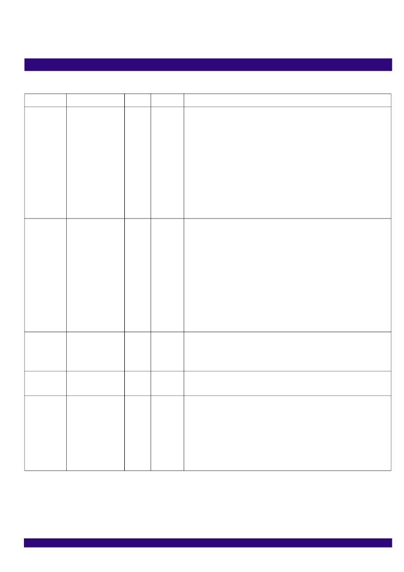
A0 / SDI
A1 / CLKE
A2
A3
A4
A5
A6
69
68
67
66
65
64
63
I
pull-down
CMOS
A[6:0]: Address Bus
In ERPOM, Intel and Motorola modes, these pins are the address bus of the microprocessor
interface.
SDI: Serial Data Input
In Serial mode, this pin is used as the serial data input. Address and data on this pin are seri-
ally clocked into the device on the rising edge of SCLK.
CLKE: SCLK Active Edge Selection
In Serial mode, this pin selects the active edge of SCLK to update the SDO:
High - The falling edge;
Low - The rising edge.
In Multiplexed mode, A0/SDI, A1/CLKE and A[6:2] pins should be connected to ground.
In Serial mode, A[6:2] pins should be connected to ground.
AD[7:0]: Address / Data Bus
In EPROM, Intel and Motorola modes, these pins are the bi-directional data bus of the micro-
processor interface.
In Multiplexed mode, these pins are the bi-directional address/data bus of the microproces-
sor interface.
AD0 / SDO
AD1
AD2
AD3
AD4
AD5
AD6
AD7
83
82
81
80
79
78
77
76
I/O
pull-down
CMOS
SDO: Serial Data Output
In Serial mode, this pin is used as the serial data output. Data on this pin is serially clocked
out of the device on the active edge of SCLK.
In Serial mode, AD[7:1] pins should be connected to ground.
WR
71
I
pull-up
CMOS
WR
: Write Operation
In Multiplexed and Intel modes, this pin is asserted low to initiate a write operation.
In Motorola mode, this pin is asserted low to initiate a write operation or s asserted high to ini-
tiate a read operation.
In EPROM and Serial modes, this pin should be connected to ground.
RD
72
I
pull-up
CMOS
RD
: Read Operation
In Multiplexed and Intel modes, this pin is asserted low to initiate a read operation.
In EPROM, Motorola and Serial modes, this pin should be connected to ground.
ALE: Address Latch Enable
In Multiplexed mode, the address on AD[7:0] pins is sampled into the device on the falling
edge of ALE.
ALE / SCLK
73
I
pull-down
CMOS
SCLK: Shift Clock
In Serial mode, a shift clock is input on this pin.
Data on SDI is sampled by the device on the rising edge of SCLK. Data on SDO is updated
on the active edge of SCLK. The active edge is determined by the CLKE.
In EPROM, Intel and Motorola modes, this pin should be connected to ground.
Table 1: Pin Description (Continued)
Name
Pin No.
I/O
Type
Description
1
相关PDF资料 |
PDF描述 |
|---|---|
| IDT82V3280PFG | WAN PLL |
| IDT82V3288 | WAN PLL |
| IDT82V3288BC | WAN PLL |
| IDT82V3288BCG | WAN PLL |
| IDT85304-01 | LOW SKEW, 1-TO-5 DIFFERENTIAL-TO-3.3V LVPECL FANOUT BUFFER |
相关代理商/技术参数 |
参数描述 |
|---|---|
| IDT82V3280PFBLANK | 制造商:IDT 制造商全称:Integrated Device Technology 功能描述:WAN PLL |
| IDT82V3280PFG | 功能描述:IC PLL WAN SE STRATUM 2 100-TQFP RoHS:是 类别:集成电路 (IC) >> 时钟/计时 - 专用 系列:- 标准包装:1,500 系列:- 类型:时钟缓冲器/驱动器 PLL:是 主要目的:- 输入:- 输出:- 电路数:- 比率 - 输入:输出:- 差分 - 输入:输出:- 频率 - 最大:- 电源电压:3.3V 工作温度:0°C ~ 70°C 安装类型:表面贴装 封装/外壳:28-SSOP(0.209",5.30mm 宽) 供应商设备封装:28-SSOP 包装:带卷 (TR) 其它名称:93786AFT |
| IDT82V3280PFG8 | 功能描述:IC PLL WAN SE STRATUM 2 100-TQFP RoHS:是 类别:集成电路 (IC) >> 时钟/计时 - 专用 系列:- 标准包装:1,500 系列:- 类型:时钟缓冲器/驱动器 PLL:是 主要目的:- 输入:- 输出:- 电路数:- 比率 - 输入:输出:- 差分 - 输入:输出:- 频率 - 最大:- 电源电压:3.3V 工作温度:0°C ~ 70°C 安装类型:表面贴装 封装/外壳:28-SSOP(0.209",5.30mm 宽) 供应商设备封装:28-SSOP 包装:带卷 (TR) 其它名称:93786AFT |
| IDT82V3280PFGBLANK | 制造商:IDT 制造商全称:Integrated Device Technology 功能描述:WAN PLL |
| IDT82V3285 | 制造商:IDT 制造商全称:Integrated Device Technology 功能描述:WAN PLL |
发布紧急采购,3分钟左右您将得到回复。