- 您现在的位置:买卖IC网 > PDF目录377488 > IDT82V3280PF (INTEGRATED DEVICE TECHNOLOGY INC) WAN PLL PDF资料下载
参数资料
| 型号: | IDT82V3280PF |
| 厂商: | INTEGRATED DEVICE TECHNOLOGY INC |
| 元件分类: | 通信及网络 |
| 英文描述: | WAN PLL |
| 中文描述: | SPECIALTY TELECOM CIRCUIT, PQFP100 |
| 封装: | TQFP-100 |
| 文件页数: | 44/167页 |
| 文件大小: | 1039K |
| 代理商: | IDT82V3280PF |
第1页第2页第3页第4页第5页第6页第7页第8页第9页第10页第11页第12页第13页第14页第15页第16页第17页第18页第19页第20页第21页第22页第23页第24页第25页第26页第27页第28页第29页第30页第31页第32页第33页第34页第35页第36页第37页第38页第39页第40页第41页第42页第43页当前第44页第45页第46页第47页第48页第49页第50页第51页第52页第53页第54页第55页第56页第57页第58页第59页第60页第61页第62页第63页第64页第65页第66页第67页第68页第69页第70页第71页第72页第73页第74页第75页第76页第77页第78页第79页第80页第81页第82页第83页第84页第85页第86页第87页第88页第89页第90页第91页第92页第93页第94页第95页第96页第97页第98页第99页第100页第101页第102页第103页第104页第105页第106页第107页第108页第109页第110页第111页第112页第113页第114页第115页第116页第117页第118页第119页第120页第121页第122页第123页第124页第125页第126页第127页第128页第129页第130页第131页第132页第133页第134页第135页第136页第137页第138页第139页第140页第141页第142页第143页第144页第145页第146页第147页第148页第149页第150页第151页第152页第153页第154页第155页第156页第157页第158页第159页第160页第161页第162页第163页第164页第165页第166页第167页
IDT82V3280
WAN PLL
Functional Description
44
June 19, 2006
3.14
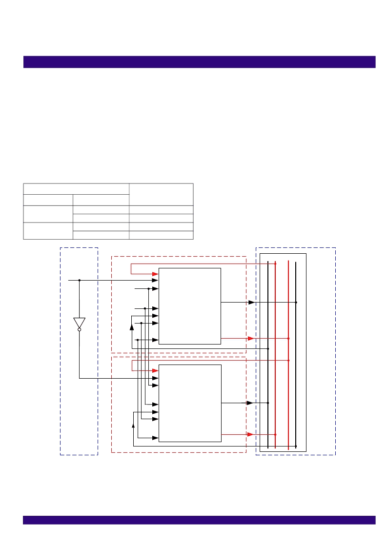
MASTER / SLAVE CONFIGURATION
Master / Slave configuration is only supported by the T0 path of the
device.
Two devices should be used together in order to:
Enable system protection against single chip failure;
Guarantee no service interrupt during system maintenance, such
as software or hardware upgrade.
Of the two devices, one is configured as the Master and the other is
configured as the Slave. The configuration is made by the MS/
SL
pin
and the MS_SL_CTRL bit (b0, 13H), as shown in
Table 29
:
In this application, all the output clocks derived from the T0 selected
input clock and the frame sync output signals from the two devices are
at the same frequency offset and phase. Refer to
Chapter 3.13.2 Frame
SYNC Output Signals
for details.
The difference between the Master and the Slave is: in the Master,
the IN11 should not be selected by the T0 DPLL; in the Slave, the follow-
ing functions are automatically forced:
The T0 selected input clock is IN11;
T0 PBO is disabled;
T0 DPLL operates at the acquisition bandwidth and damping fac-
tor;
EX_SYNC1 is used for synchronization;
T0 DPLL operates in Locked mode.
In the Slave, the corresponding registers of the above forced func-
tions can still be configured, but their configuration does not take any
effect. The frequency of the T0 selected input clock IN11 is recom-
mended to be 6.48 MHz.
Figure 13. Physical Connection Between Two Devices
Table 29: Device Master / Slave Control
Master / Slave Control
Result
MS/
SL
pin
MS_SL_CTRL Bit
High
0
1
0
1
Master
Slave
Slave
Master
Low
MS/
SL
IN1
.
.
.
one output
clock
Hardware
control
IN10
IN11
IN12
IN14
.
one output
frame sync
signal
OUT1
OUT2
FRSYNC_8K/
MFRSYNC_2K
OUT7
.
.
.
.
.
.
MS/
SL
IN1
.
.
IN10
IN11
IN12
IN14
.
.
OUT1
OUT2
FRSYNC_8K/
MFRSYNC_2K
OUT7
.
.
.
.
.
Backplane connections
EX_SYNC1
EX_SYNC1
Chip A
Backplane
Backplane
Chip B
.
.
.
.
.
.
.
.
.
.
.
.
one output
clock
one output
frame sync
signal
相关PDF资料 |
PDF描述 |
|---|---|
| IDT82V3280PFG | WAN PLL |
| IDT82V3288 | WAN PLL |
| IDT82V3288BC | WAN PLL |
| IDT82V3288BCG | WAN PLL |
| IDT85304-01 | LOW SKEW, 1-TO-5 DIFFERENTIAL-TO-3.3V LVPECL FANOUT BUFFER |
相关代理商/技术参数 |
参数描述 |
|---|---|
| IDT82V3280PFBLANK | 制造商:IDT 制造商全称:Integrated Device Technology 功能描述:WAN PLL |
| IDT82V3280PFG | 功能描述:IC PLL WAN SE STRATUM 2 100-TQFP RoHS:是 类别:集成电路 (IC) >> 时钟/计时 - 专用 系列:- 标准包装:1,500 系列:- 类型:时钟缓冲器/驱动器 PLL:是 主要目的:- 输入:- 输出:- 电路数:- 比率 - 输入:输出:- 差分 - 输入:输出:- 频率 - 最大:- 电源电压:3.3V 工作温度:0°C ~ 70°C 安装类型:表面贴装 封装/外壳:28-SSOP(0.209",5.30mm 宽) 供应商设备封装:28-SSOP 包装:带卷 (TR) 其它名称:93786AFT |
| IDT82V3280PFG8 | 功能描述:IC PLL WAN SE STRATUM 2 100-TQFP RoHS:是 类别:集成电路 (IC) >> 时钟/计时 - 专用 系列:- 标准包装:1,500 系列:- 类型:时钟缓冲器/驱动器 PLL:是 主要目的:- 输入:- 输出:- 电路数:- 比率 - 输入:输出:- 差分 - 输入:输出:- 频率 - 最大:- 电源电压:3.3V 工作温度:0°C ~ 70°C 安装类型:表面贴装 封装/外壳:28-SSOP(0.209",5.30mm 宽) 供应商设备封装:28-SSOP 包装:带卷 (TR) 其它名称:93786AFT |
| IDT82V3280PFGBLANK | 制造商:IDT 制造商全称:Integrated Device Technology 功能描述:WAN PLL |
| IDT82V3285 | 制造商:IDT 制造商全称:Integrated Device Technology 功能描述:WAN PLL |
发布紧急采购,3分钟左右您将得到回复。