- 您现在的位置:买卖IC网 > PDF目录2081 > ISPPAC-CLK5320S-01T64I (Lattice Semiconductor Corporation)IC BUFFER FANOUT ISP UNIV 64TQFP PDF资料下载
参数资料
| 型号: | ISPPAC-CLK5320S-01T64I |
| 厂商: | Lattice Semiconductor Corporation |
| 文件页数: | 26/56页 |
| 文件大小: | 0K |
| 描述: | IC BUFFER FANOUT ISP UNIV 64TQFP |
| 标准包装: | 160 |
| 系列: | ispClock™ |
| 类型: | 时钟发生器,扇出配送,零延迟缓冲器 |
| PLL: | 带旁路 |
| 输入: | HSTL,LVCMOS,LVDS,LVPECL,LVTTL,SSTL |
| 输出: | eHSTL,HSTL,LVCMOS,LVTTL,SSTL |
| 电路数: | 1 |
| 比率 - 输入:输出: | 2:20 |
| 差分 - 输入:输出: | 是/无 |
| 频率 - 最大: | 267MHz |
| 除法器/乘法器: | 是/无 |
| 电源电压: | 3 V ~ 3.6 V |
| 工作温度: | -40°C ~ 85°C |
| 安装类型: | 表面贴装 |
| 封装/外壳: | 64-LQFP |
| 供应商设备封装: | 64-TQFP(10x10) |
| 包装: | 托盘 |
第1页第2页第3页第4页第5页第6页第7页第8页第9页第10页第11页第12页第13页第14页第15页第16页第17页第18页第19页第20页第21页第22页第23页第24页第25页当前第26页第27页第28页第29页第30页第31页第32页第33页第34页第35页第36页第37页第38页第39页第40页第41页第42页第43页第44页第45页第46页第47页第48页第49页第50页第51页第52页第53页第54页第55页第56页
Lattice Semiconductor
ispClock5300S Family Data Sheet
32
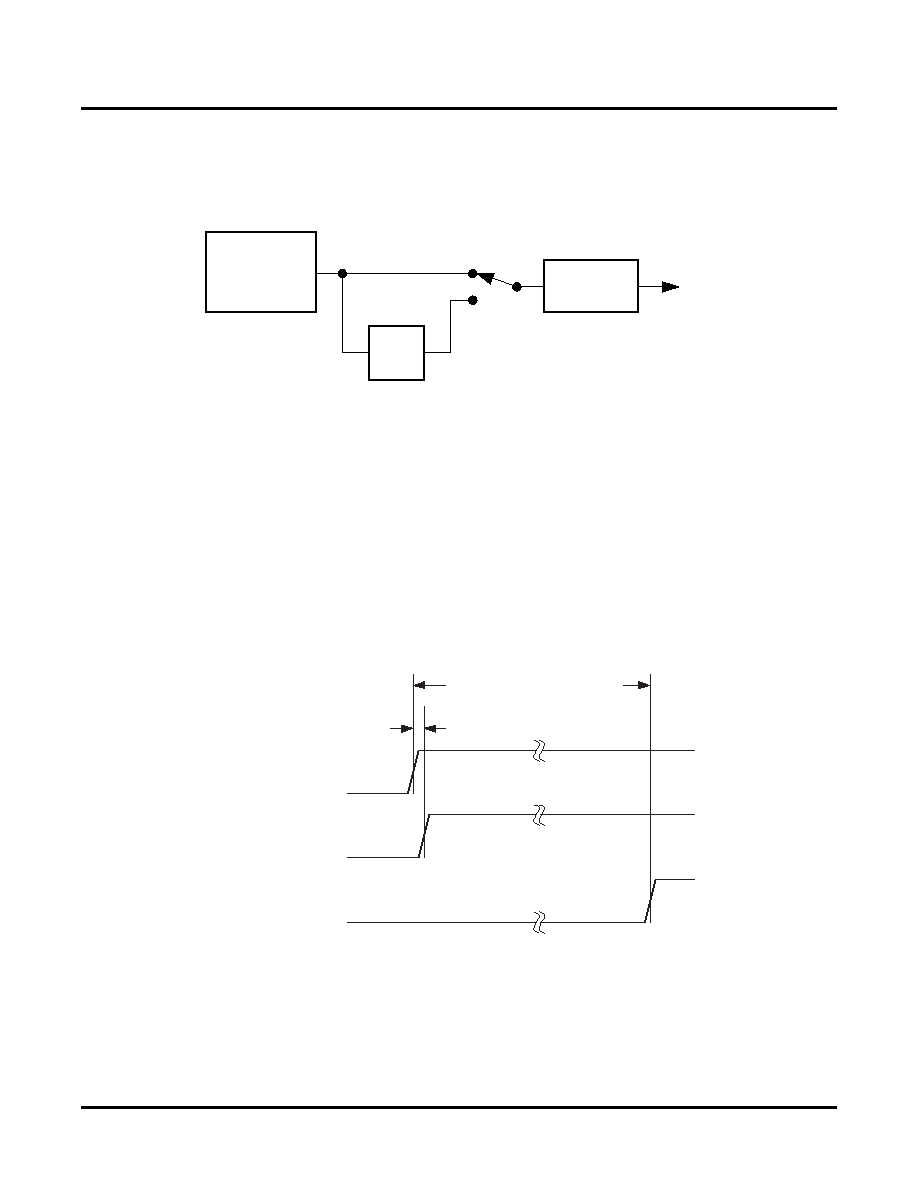
(fVCO = 400MHz) to 780ps (fVCO = 160MHz), which is twice as long as those provided in ne skew mode. When
coarse skew mode is selected, an additional divide-by-2 stage is effectively inserted between the VCO and the V-
divider bank, as shown in Figure 26. When assigning divider settings in coarse skew mode, one must account for
this additional divide-by-two so that the VCO still operates within its specied range (160-400MHz).
Figure 26. Additional Factor-of-2 Division in Coarse Mode
When one moves from ne skew mode to coarse skew mode with a given divider conguration, the VCO frequency
will attempt to double to compensate for the additional divide-by-2 stage. Because the fVCO range is not increased,
however, one must modify the feedback path V-divider settings to bring fVCO back into its specied operating range
(160MHz to 400MHz). This can be accomplished by dividing all V-divider settings by two. All output frequencies will
remain unchanged from what they were in ne mode.
Output Skew Matching and Accuracy
Understanding the various factors which relate to output skew is essential for realizing optimal skew performance in
the ispClock5300S family of devices.
In the case where two outputs are identically congured, and driving identical loads, the maximum skew is dened
by tSKEW, which is specied as a maximum of 100ps. In Figure 27 the Bank1A and BANK2A outputs show the skew
error between two matched outputs.
Figure 27. Skew Matching Error Sources
One can also program a user-dened skew between two outputs using the skew control units. Because the pro-
grammable skew is derived from the VCO frequency, as described in the previous section, the absolute skew is
very accurate. The typical error for any non-zero skew setting is given by the tSKERR specication. For example, if
one is in ne skew mode with a VCO frequency of 250MHz, and selects a skew of 4TU, the realized skew will be
1ns, which will typically be accurate to within +/-30 ps. An example of error vs. skew setting can be found in the
chart ‘Typical Skew Error vs. Setting’ in the typical performance characteristics section. Note that this parameter
adds to output-to-output skew error only if the two outputs have different skew settings. The Bank1A and Bank3A
VCO
÷2
V-dividers
Fine
Mode
Fout
Coarse
Mode
+/- t
SKEW
1ns +/- (t
SKEW) +/- (tSKERR)
BANK1A
(skew setting = 0)
BANK2A
(skew setting=0)
BANK3A
(skew setting = 1ns)
相关PDF资料 |
PDF描述 |
|---|---|
| KA2901DMTF | IC COMPARATOR QUAD 14-SOP |
| KA319 | IC COMPARATOR DUAL HS 14-DIP |
| KA393D | IC COMPARATOR DUAL DIFF 8-SOP |
| LA42032-E | IC AF POWER AMP 5WX2CH SIP13H |
| LA4425A-E | IC AUDIO POWER AMP 5W TO-126ML |
相关代理商/技术参数 |
参数描述 |
|---|---|
| ISPPACCLK5320S-01T64I | 制造商:LATTICE 制造商全称:Lattice Semiconductor 功能描述:In-System Programmable, Zero-Delay, Universal Fan-Out Buffer, Single-Ended |
| ISPPACCLK5320S-01TN48C | 制造商:LATTICE 制造商全称:Lattice Semiconductor 功能描述:In-System Programmable, Zero-Delay, Universal Fan-Out Buffer, Single-Ended |
| ISPPACCLK5320S-01TN48I | 制造商:LATTICE 制造商全称:Lattice Semiconductor 功能描述:In-System Programmable, Zero-Delay, Universal Fan-Out Buffer, Single-Ended |
| ispPAC-CLK5320S-01TN64C | 功能描述:时钟驱动器及分配 ISP 0 Delay Unv Fan- Out Buf-Sngl End RoHS:否 制造商:Micrel 乘法/除法因子:1:4 输出类型:Differential 最大输出频率:4.2 GHz 电源电压-最大: 电源电压-最小:5 V 最大工作温度:+ 85 C 封装 / 箱体:SOIC-8 封装:Reel |
| ISPPACCLK5320S-01TN64C | 制造商:LATTICE 制造商全称:Lattice Semiconductor 功能描述:In-System Programmable, Zero-Delay, Universal Fan-Out Buffer, Single-Ended |
发布紧急采购,3分钟左右您将得到回复。