- 您现在的位置:买卖IC网 > PDF目录2081 > ISPPAC-CLK5320S-01T64I (Lattice Semiconductor Corporation)IC BUFFER FANOUT ISP UNIV 64TQFP PDF资料下载
参数资料
| 型号: | ISPPAC-CLK5320S-01T64I |
| 厂商: | Lattice Semiconductor Corporation |
| 文件页数: | 27/56页 |
| 文件大小: | 0K |
| 描述: | IC BUFFER FANOUT ISP UNIV 64TQFP |
| 标准包装: | 160 |
| 系列: | ispClock™ |
| 类型: | 时钟发生器,扇出配送,零延迟缓冲器 |
| PLL: | 带旁路 |
| 输入: | HSTL,LVCMOS,LVDS,LVPECL,LVTTL,SSTL |
| 输出: | eHSTL,HSTL,LVCMOS,LVTTL,SSTL |
| 电路数: | 1 |
| 比率 - 输入:输出: | 2:20 |
| 差分 - 输入:输出: | 是/无 |
| 频率 - 最大: | 267MHz |
| 除法器/乘法器: | 是/无 |
| 电源电压: | 3 V ~ 3.6 V |
| 工作温度: | -40°C ~ 85°C |
| 安装类型: | 表面贴装 |
| 封装/外壳: | 64-LQFP |
| 供应商设备封装: | 64-TQFP(10x10) |
| 包装: | 托盘 |
第1页第2页第3页第4页第5页第6页第7页第8页第9页第10页第11页第12页第13页第14页第15页第16页第17页第18页第19页第20页第21页第22页第23页第24页第25页第26页当前第27页第28页第29页第30页第31页第32页第33页第34页第35页第36页第37页第38页第39页第40页第41页第42页第43页第44页第45页第46页第47页第48页第49页第50页第51页第52页第53页第54页第55页第56页
Lattice Semiconductor
ispClock5300S Family Data Sheet
33
outputs in Figure 27 show how the various sources of skew error stack up in this case. Note that if two or more out-
puts are programmed to the same skew setting, then the contribution of the tSKERR skew error term does not apply.
When outputs are congured or loaded differently, this also has an effect on skew matching. If an output is set to
support a different logic type, this can be accounted for by using the t(ioo) output adders specied in the table
‘Switching Characteristics’. That table species the additional skew added to an output using SSTL, HSTL, EHSTL
as a base-line. For instance, if one output is specied as LVTTL, it has a delay adder relative to SSTL of 0.25ns. If
another output is specied as SSTL3, then one would expect 0.25ns of additional skew between the two outputs
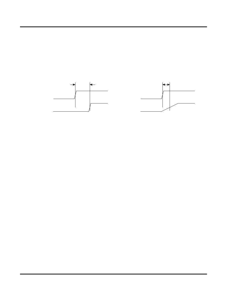
due to this adder. This timing relationship is shown in Figure 28a.
Figure 28. Output Timing Adders for Logic Type (a) and Output Slew Rate (b)
By selecting the same feedback logic type and clock output, the output delay adders for the clock output are auto-
matically compensated for. Similarly, a reference clock delay adder can be compensated for by selecting the same
feedback input logic type and reference clock.
When the internal feedback mode is selected, however, one should add both input and output delay adders to tDELAY
specied in the Performance Characteristics PLL table to calculate the input-to-output delay.
Similarly, when one changes the slew rate of an output, the output slew rate adders (tIOS) can be used to predict
the resulting skew. In this case, the fastest slew setting (1) is used as the baseline against which other slews are
measured. For example, in the case of outputs congured to the same logic type (e.g. LVCMOS 1.8V), if one output
is set to the fastest slew rate (1, tIOS = 0ps), and another set to slew rate 3 (tIOS = 950ps), then one could expect
950ps of skew between the two outputs, as shown in Figure 28b.
Static Phase Offset and Input-Output Skew
The ispClock5300S’s external feedback inputs can be used to obtain near-zero effective delays from the clock ref-
erence input pins to a designated output pin. Using external feedback (Figure 29), the PLL will attempt to force the
output phase so that the rising edge phase (tφ) at the feedback input matches the rising edge phase at the refer-
ence input. The residual error between the two is specied as the static phase error. Note that any propagation
delay (tFBK) in the external feedback path drives the phase of the output signal backwards in time as measured at
the output. For this reason, if zero input-to-output delays are required, the length of the signal path between the
output pin and the feedback pin should be minimized.
SSTL3 Output
LVTTL Output
0.25ns
(a)
LVCMOS Output
(Slew rate=1)
LVCMOS Output
(Slew rate=3)
950ps
(b)
相关PDF资料 |
PDF描述 |
|---|---|
| KA2901DMTF | IC COMPARATOR QUAD 14-SOP |
| KA319 | IC COMPARATOR DUAL HS 14-DIP |
| KA393D | IC COMPARATOR DUAL DIFF 8-SOP |
| LA42032-E | IC AF POWER AMP 5WX2CH SIP13H |
| LA4425A-E | IC AUDIO POWER AMP 5W TO-126ML |
相关代理商/技术参数 |
参数描述 |
|---|---|
| ISPPACCLK5320S-01T64I | 制造商:LATTICE 制造商全称:Lattice Semiconductor 功能描述:In-System Programmable, Zero-Delay, Universal Fan-Out Buffer, Single-Ended |
| ISPPACCLK5320S-01TN48C | 制造商:LATTICE 制造商全称:Lattice Semiconductor 功能描述:In-System Programmable, Zero-Delay, Universal Fan-Out Buffer, Single-Ended |
| ISPPACCLK5320S-01TN48I | 制造商:LATTICE 制造商全称:Lattice Semiconductor 功能描述:In-System Programmable, Zero-Delay, Universal Fan-Out Buffer, Single-Ended |
| ispPAC-CLK5320S-01TN64C | 功能描述:时钟驱动器及分配 ISP 0 Delay Unv Fan- Out Buf-Sngl End RoHS:否 制造商:Micrel 乘法/除法因子:1:4 输出类型:Differential 最大输出频率:4.2 GHz 电源电压-最大: 电源电压-最小:5 V 最大工作温度:+ 85 C 封装 / 箱体:SOIC-8 封装:Reel |
| ISPPACCLK5320S-01TN64C | 制造商:LATTICE 制造商全称:Lattice Semiconductor 功能描述:In-System Programmable, Zero-Delay, Universal Fan-Out Buffer, Single-Ended |
发布紧急采购,3分钟左右您将得到回复。