- 您现在的位置:买卖IC网 > PDF目录2081 > ISPPAC-CLK5320S-01T64I (Lattice Semiconductor Corporation)IC BUFFER FANOUT ISP UNIV 64TQFP PDF资料下载
参数资料
| 型号: | ISPPAC-CLK5320S-01T64I |
| 厂商: | Lattice Semiconductor Corporation |
| 文件页数: | 30/56页 |
| 文件大小: | 0K |
| 描述: | IC BUFFER FANOUT ISP UNIV 64TQFP |
| 标准包装: | 160 |
| 系列: | ispClock™ |
| 类型: | 时钟发生器,扇出配送,零延迟缓冲器 |
| PLL: | 带旁路 |
| 输入: | HSTL,LVCMOS,LVDS,LVPECL,LVTTL,SSTL |
| 输出: | eHSTL,HSTL,LVCMOS,LVTTL,SSTL |
| 电路数: | 1 |
| 比率 - 输入:输出: | 2:20 |
| 差分 - 输入:输出: | 是/无 |
| 频率 - 最大: | 267MHz |
| 除法器/乘法器: | 是/无 |
| 电源电压: | 3 V ~ 3.6 V |
| 工作温度: | -40°C ~ 85°C |
| 安装类型: | 表面贴装 |
| 封装/外壳: | 64-LQFP |
| 供应商设备封装: | 64-TQFP(10x10) |
| 包装: | 托盘 |
第1页第2页第3页第4页第5页第6页第7页第8页第9页第10页第11页第12页第13页第14页第15页第16页第17页第18页第19页第20页第21页第22页第23页第24页第25页第26页第27页第28页第29页当前第30页第31页第32页第33页第34页第35页第36页第37页第38页第39页第40页第41页第42页第43页第44页第45页第46页第47页第48页第49页第50页第51页第52页第53页第54页第55页第56页
Lattice Semiconductor
ispClock5300S Family Data Sheet
36
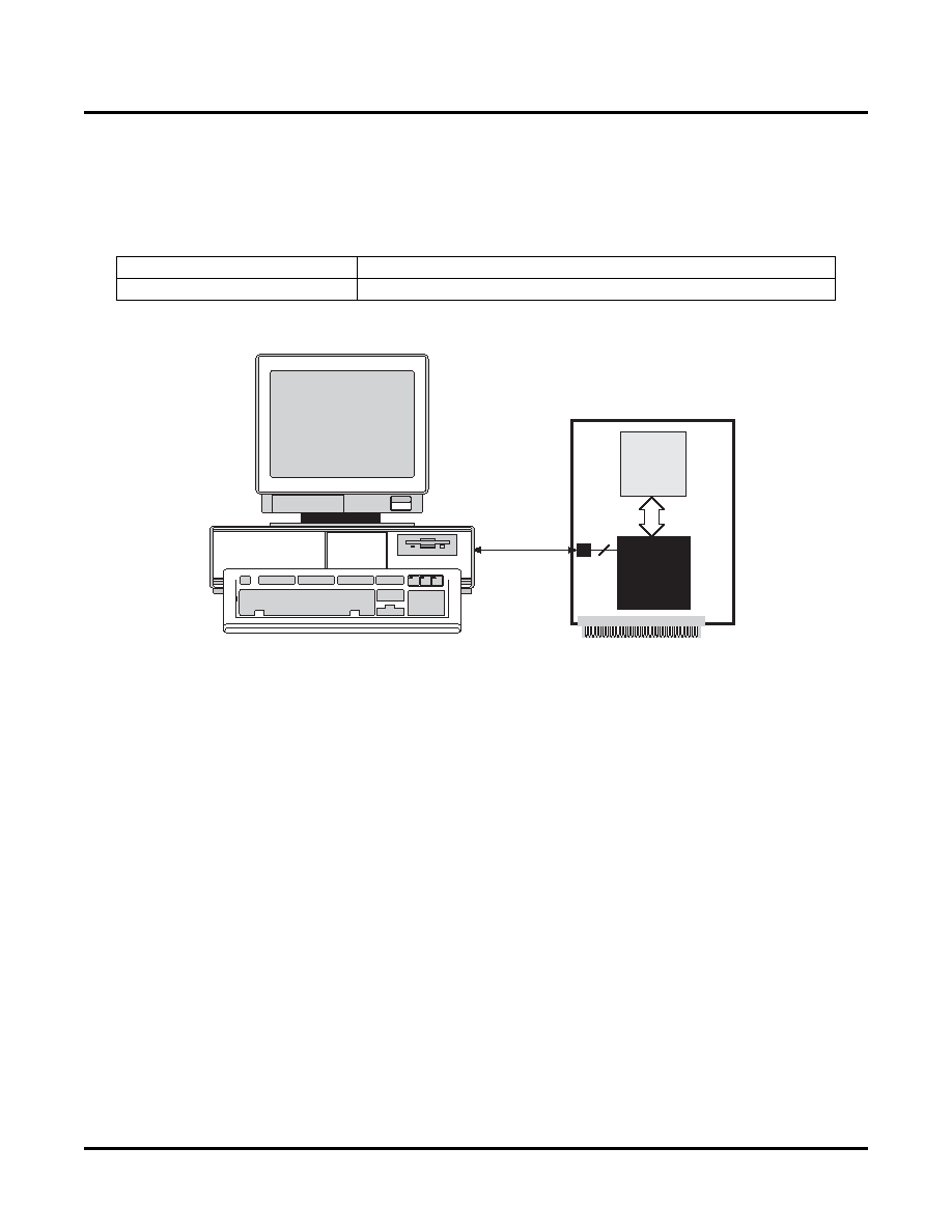
Evaluation Fixture
Included in the basic ispClock5300S Design Kit is an engineering prototype board that can be connected to the
parallel port of a PC using a Lattice ispDOWNLOAD
cable. It demonstrates proper layout techniques for the
ispClock5300S and can be used in real time to check circuit operation as part of the design process. Input and out-
put connections (SMA connectors for all RF signals) are provided to aid in the evaluation of the ispClock5300S for
a given application. (Figure 31).
Figure 31. Download from a PC
IEEE Standard 1149.1 Interface (JTAG)
Serial Port Programming Interface Communication with the ispClock5300S is facilitated via an IEEE 1149.1 test
access port (TAP). It is used by the ispClock5300S both as a serial programming interface, and for boundary scan
test purposes. A brief description of the ispClock5300S JTAG interface follows. For complete details of the refer-
ence specication, refer to the publication, Standard Test Access Port and Boundary-Scan Architecture, IEEE Std.
1149.1-1990 (which now includes IEEE Std. 1149.1a-1993).
Overview
An IEEE 1149.1 test access port (TAP) provides the control interface for serially accessing the digital I/O of the
ispClock5300S. The TAP controller is a state machine driven with mode and clock inputs. Given in the correct
sequence, instructions are shifted into an instruction register which then determines subsequent data input, data
output, and related operations. Device programming is performed by addressing the conguration register, shifting
data in, and then executing a program conguration instruction, after which the data is transferred to internal
E
2CMOS cells. It is these non-volatile cells that store the conguration of the ispClock5300S. A set of instructions
are dened that access all data registers and perform other internal control operations. For compatibility between
compliant devices, two data registers are mandated by the IEEE 1149.1 specication. Others are functionally spec-
ied, but inclusion is strictly optional. Finally, there are provisions for optional data registers dened by the manu-
facturer. The two required registers are the bypass and boundary-scan registers. Figure 32 shows how the
instruction and various data registers are organized in an ispClock5300S.
Part Number
Description
PAC-SYSTEMCLK5312S
Complete system kit, evaluation board, ispDOWNLOAD cable and software.
ispDownload
Cable (6')
4
Other
System
Circuitry
ispClock5300S
Device
PAC-Designer
Software
相关PDF资料 |
PDF描述 |
|---|---|
| KA2901DMTF | IC COMPARATOR QUAD 14-SOP |
| KA319 | IC COMPARATOR DUAL HS 14-DIP |
| KA393D | IC COMPARATOR DUAL DIFF 8-SOP |
| LA42032-E | IC AF POWER AMP 5WX2CH SIP13H |
| LA4425A-E | IC AUDIO POWER AMP 5W TO-126ML |
相关代理商/技术参数 |
参数描述 |
|---|---|
| ISPPACCLK5320S-01T64I | 制造商:LATTICE 制造商全称:Lattice Semiconductor 功能描述:In-System Programmable, Zero-Delay, Universal Fan-Out Buffer, Single-Ended |
| ISPPACCLK5320S-01TN48C | 制造商:LATTICE 制造商全称:Lattice Semiconductor 功能描述:In-System Programmable, Zero-Delay, Universal Fan-Out Buffer, Single-Ended |
| ISPPACCLK5320S-01TN48I | 制造商:LATTICE 制造商全称:Lattice Semiconductor 功能描述:In-System Programmable, Zero-Delay, Universal Fan-Out Buffer, Single-Ended |
| ispPAC-CLK5320S-01TN64C | 功能描述:时钟驱动器及分配 ISP 0 Delay Unv Fan- Out Buf-Sngl End RoHS:否 制造商:Micrel 乘法/除法因子:1:4 输出类型:Differential 最大输出频率:4.2 GHz 电源电压-最大: 电源电压-最小:5 V 最大工作温度:+ 85 C 封装 / 箱体:SOIC-8 封装:Reel |
| ISPPACCLK5320S-01TN64C | 制造商:LATTICE 制造商全称:Lattice Semiconductor 功能描述:In-System Programmable, Zero-Delay, Universal Fan-Out Buffer, Single-Ended |
发布紧急采购,3分钟左右您将得到回复。