- 您现在的位置:买卖IC网 > PDF目录2081 > ISPPAC-CLK5320S-01T64I (Lattice Semiconductor Corporation)IC BUFFER FANOUT ISP UNIV 64TQFP PDF资料下载
参数资料
| 型号: | ISPPAC-CLK5320S-01T64I |
| 厂商: | Lattice Semiconductor Corporation |
| 文件页数: | 32/56页 |
| 文件大小: | 0K |
| 描述: | IC BUFFER FANOUT ISP UNIV 64TQFP |
| 标准包装: | 160 |
| 系列: | ispClock™ |
| 类型: | 时钟发生器,扇出配送,零延迟缓冲器 |
| PLL: | 带旁路 |
| 输入: | HSTL,LVCMOS,LVDS,LVPECL,LVTTL,SSTL |
| 输出: | eHSTL,HSTL,LVCMOS,LVTTL,SSTL |
| 电路数: | 1 |
| 比率 - 输入:输出: | 2:20 |
| 差分 - 输入:输出: | 是/无 |
| 频率 - 最大: | 267MHz |
| 除法器/乘法器: | 是/无 |
| 电源电压: | 3 V ~ 3.6 V |
| 工作温度: | -40°C ~ 85°C |
| 安装类型: | 表面贴装 |
| 封装/外壳: | 64-LQFP |
| 供应商设备封装: | 64-TQFP(10x10) |
| 包装: | 托盘 |
第1页第2页第3页第4页第5页第6页第7页第8页第9页第10页第11页第12页第13页第14页第15页第16页第17页第18页第19页第20页第21页第22页第23页第24页第25页第26页第27页第28页第29页第30页第31页当前第32页第33页第34页第35页第36页第37页第38页第39页第40页第41页第42页第43页第44页第45页第46页第47页第48页第49页第50页第51页第52页第53页第54页第55页第56页
Lattice Semiconductor
ispClock5300S Family Data Sheet
38
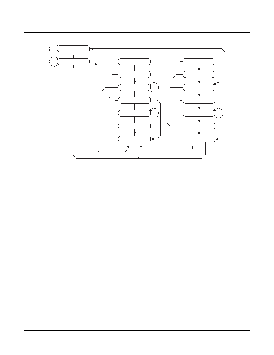
Figure 33. TAP States
When the correct logic sequence is applied to the TMS and TCK inputs, the TAP will exit the Test-Logic-Reset state
and move to the desired state. The next state after Test-Logic-Reset is Run-Test/Idle. Until a data or instruction shift
is performed, no action will occur in Run-Test/Idle (steady state = idle). After Run-Test/Idle, either a data or instruc-
tion shift is performed. The states of the Data and Instruction Register blocks are identical to each other differing
only in their entry points. When either block is entered, the rst action is a capture operation. For the Data Regis-
ters, the Capture-DR state is very simple: it captures (parallel loads) data onto the selected serial data path (previ-
ously chosen with the appropriate instruction). For the Instruction Register, the Capture-IR state will always load
the IDCODE instruction. It will always enable the ID Register for readout if no other instruction is loaded prior to a
Shift-DR operation. This, in conjunction with mandated bit codes, allows a “blind” interrogation of any device in a
compliant IEEE 1149.1 serial chain. From the Capture state, the TAP transitions to either the Shift or Exit1 state.
Normally the Shift state follows the Capture state so that test data or status information can be shifted out or new
data shifted in. Following the Shift state, the TAP either returns to the Run-Test/Idle state via the Exit1 and Update
states or enters the Pause state via Exit1. The Pause state is used to temporarily suspend the shifting of data
through either the Data or Instruction Register while an external operation is performed. From the Pause state,
shifting can resume by reentering the Shift state via the Exit2 state or be terminated by entering the Run-Test/Idle
state via the Exit2 and Update states. If the proper instruction is shifted in during a Shift-IR operation, the next entry
into Run-Test/Idle initiates the test mode (steady state = test). This is when the device is actually programmed,
erased or veried. All other instructions are executed in the Update state.
Test Instructions
Like data registers, the IEEE 1149.1 standard also mandates the inclusion of certain instructions. It outlines the
function of three required and six optional instructions. Any additional instructions are left exclusively for the manu-
facturer to determine. The instruction word length is not mandated other than to be a minimum of two bits, with only
the BYPASS and EXTEST instruction code patterns being specically called out (all ones and all zeroes respec-
tively). The ispClock5300S contains the required minimum instruction set as well as one from the optional instruc-
tion set. In addition, there are several proprietary instructions that allow the device to be congured and veried.
Test-Logic-Rst
Run-Test/Idle
Select-DR-Scan
Select-IR-Scan
Capture-DR
Capture-IR
Shift-DR
Shift-IR
Exit1-DR
Exit1-IR
Pause-DR
Pause-IR
Exit2-DR
Exit2-IR
Update-DR
Update-IR
1
0
00
0
00
11
00
11
00
11
00
11
1
0
Note: The value shown adjacent to each state transition in this figure
represents the signal present at TMS at the time of a rising edge at TCK.
相关PDF资料 |
PDF描述 |
|---|---|
| KA2901DMTF | IC COMPARATOR QUAD 14-SOP |
| KA319 | IC COMPARATOR DUAL HS 14-DIP |
| KA393D | IC COMPARATOR DUAL DIFF 8-SOP |
| LA42032-E | IC AF POWER AMP 5WX2CH SIP13H |
| LA4425A-E | IC AUDIO POWER AMP 5W TO-126ML |
相关代理商/技术参数 |
参数描述 |
|---|---|
| ISPPACCLK5320S-01T64I | 制造商:LATTICE 制造商全称:Lattice Semiconductor 功能描述:In-System Programmable, Zero-Delay, Universal Fan-Out Buffer, Single-Ended |
| ISPPACCLK5320S-01TN48C | 制造商:LATTICE 制造商全称:Lattice Semiconductor 功能描述:In-System Programmable, Zero-Delay, Universal Fan-Out Buffer, Single-Ended |
| ISPPACCLK5320S-01TN48I | 制造商:LATTICE 制造商全称:Lattice Semiconductor 功能描述:In-System Programmable, Zero-Delay, Universal Fan-Out Buffer, Single-Ended |
| ispPAC-CLK5320S-01TN64C | 功能描述:时钟驱动器及分配 ISP 0 Delay Unv Fan- Out Buf-Sngl End RoHS:否 制造商:Micrel 乘法/除法因子:1:4 输出类型:Differential 最大输出频率:4.2 GHz 电源电压-最大: 电源电压-最小:5 V 最大工作温度:+ 85 C 封装 / 箱体:SOIC-8 封装:Reel |
| ISPPACCLK5320S-01TN64C | 制造商:LATTICE 制造商全称:Lattice Semiconductor 功能描述:In-System Programmable, Zero-Delay, Universal Fan-Out Buffer, Single-Ended |
发布紧急采购,3分钟左右您将得到回复。