- 您现在的位置:买卖IC网 > PDF目录2081 > ISPPAC-CLK5320S-01T64I (Lattice Semiconductor Corporation)IC BUFFER FANOUT ISP UNIV 64TQFP PDF资料下载
参数资料
| 型号: | ISPPAC-CLK5320S-01T64I |
| 厂商: | Lattice Semiconductor Corporation |
| 文件页数: | 3/56页 |
| 文件大小: | 0K |
| 描述: | IC BUFFER FANOUT ISP UNIV 64TQFP |
| 标准包装: | 160 |
| 系列: | ispClock™ |
| 类型: | 时钟发生器,扇出配送,零延迟缓冲器 |
| PLL: | 带旁路 |
| 输入: | HSTL,LVCMOS,LVDS,LVPECL,LVTTL,SSTL |
| 输出: | eHSTL,HSTL,LVCMOS,LVTTL,SSTL |
| 电路数: | 1 |
| 比率 - 输入:输出: | 2:20 |
| 差分 - 输入:输出: | 是/无 |
| 频率 - 最大: | 267MHz |
| 除法器/乘法器: | 是/无 |
| 电源电压: | 3 V ~ 3.6 V |
| 工作温度: | -40°C ~ 85°C |
| 安装类型: | 表面贴装 |
| 封装/外壳: | 64-LQFP |
| 供应商设备封装: | 64-TQFP(10x10) |
| 包装: | 托盘 |
第1页第2页当前第3页第4页第5页第6页第7页第8页第9页第10页第11页第12页第13页第14页第15页第16页第17页第18页第19页第20页第21页第22页第23页第24页第25页第26页第27页第28页第29页第30页第31页第32页第33页第34页第35页第36页第37页第38页第39页第40页第41页第42页第43页第44页第45页第46页第47页第48页第49页第50页第51页第52页第53页第54页第55页第56页
Lattice Semiconductor
ispClock5300S Family Data Sheet
11
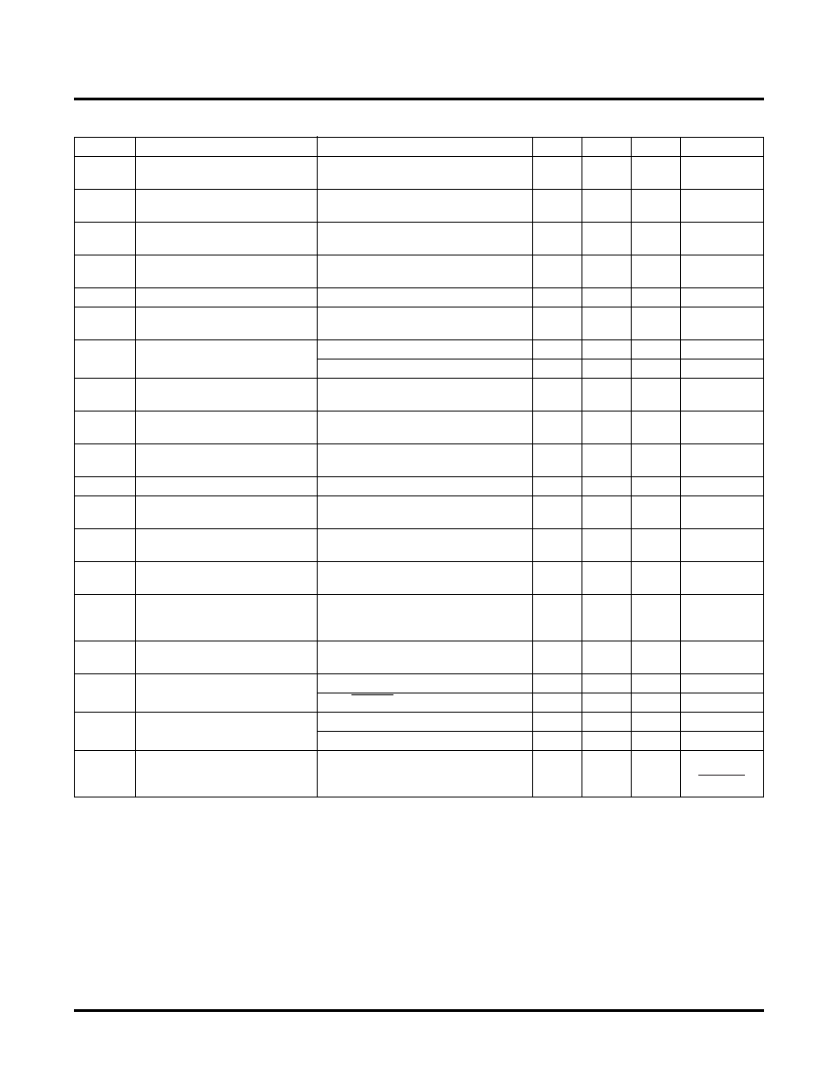
Performance Characteristics – PLL
Symbol
Parameter
Conditions
Min.
Typ.
Max.
Units
fREF, fFBK
Reference and feedback input
frequency range
8
267
MHz
tCLOCKHI,
tCLOCKLO
Reference and feedback input
clock HIGH and LOW times
1.25
ns
tRINP,
tFINP
Reference and feedback input
rise and fall times
Measured between 20% and 80%
levels
5ns
fPFD
Phase detector input frequency
range
8
267
MHz
fVCO
VCO operating frequency
160
400
MHz
VDIV
Output divider range (Power of
2)
132
fOUT
Output frequency range
1
Fine Skew Mode
5
267
MHz
Coarse Skew Mode
2.5
200
MHz
tJIT (cc)
Output adjacent-cycle jitter
5
(1000 cycle sample)
fPFD ≥ 100MHz
70
ps (p-p)
tJIT (per)
Output period jitter
5
(10000 cycle sample)
fPFD ≥ 100MHz
9
ps (RMS)
tJIT(φ)
Reference clock to output jitter
5
(2000 cycle sample)
fPFD ≥ 100MHz
50
ps (RMS)
tφ
Static phase offset
4
PFD input frequency ≥100MHz
3
-40
100
ps
tφDYN
Dynamic phase offset
100MHz, Spread Spectrum
Modulation index = 0.5%
28
ps
DCERR
Output duty cycle error
Output type LVCMOS 3.3V
2
fOUT >100 MHz
47
53
%
tPDBYPASS
Reference clock to output
propagation delay
V=1
6.5
ns
tPD_FOB
Reference to output propagation
delay in Non-Zero Delay Buffer
Mode
V=1
2.5
3.5
5
ns
tDELAY
Reference to output delay with
internal feedback mode
3
V=1
500
ps
tLOCK
PLL lock time
From Power-up event
150
s
From RESET event
15
s
tRELOCK
PLL relock time
To same reference frequency
15
s
To different frequency
150
s
PSR
Power supply rejection, period
jitter vs. power supply noise
fIN = fOUT = 100MHz
VCCA = VCCD = VCCO modulated with
100kHz sinusoidal stimulus
0.05
1. In PLL Bypass mode (PLL_BYPASS = HIGH), output will support frequencies down to 0Hz (divider chain is a fully static design).
3. Input and outputs LVCMOS mode
4. Inserted feedback loop delay < 7ns
5. Measured with fOUT = 100MHz, fVCO = 400MHz, input and output interface set to LVCMOS.
ps(RMS)
mV(p-p)
相关PDF资料 |
PDF描述 |
|---|---|
| KA2901DMTF | IC COMPARATOR QUAD 14-SOP |
| KA319 | IC COMPARATOR DUAL HS 14-DIP |
| KA393D | IC COMPARATOR DUAL DIFF 8-SOP |
| LA42032-E | IC AF POWER AMP 5WX2CH SIP13H |
| LA4425A-E | IC AUDIO POWER AMP 5W TO-126ML |
相关代理商/技术参数 |
参数描述 |
|---|---|
| ISPPACCLK5320S-01T64I | 制造商:LATTICE 制造商全称:Lattice Semiconductor 功能描述:In-System Programmable, Zero-Delay, Universal Fan-Out Buffer, Single-Ended |
| ISPPACCLK5320S-01TN48C | 制造商:LATTICE 制造商全称:Lattice Semiconductor 功能描述:In-System Programmable, Zero-Delay, Universal Fan-Out Buffer, Single-Ended |
| ISPPACCLK5320S-01TN48I | 制造商:LATTICE 制造商全称:Lattice Semiconductor 功能描述:In-System Programmable, Zero-Delay, Universal Fan-Out Buffer, Single-Ended |
| ispPAC-CLK5320S-01TN64C | 功能描述:时钟驱动器及分配 ISP 0 Delay Unv Fan- Out Buf-Sngl End RoHS:否 制造商:Micrel 乘法/除法因子:1:4 输出类型:Differential 最大输出频率:4.2 GHz 电源电压-最大: 电源电压-最小:5 V 最大工作温度:+ 85 C 封装 / 箱体:SOIC-8 封装:Reel |
| ISPPACCLK5320S-01TN64C | 制造商:LATTICE 制造商全称:Lattice Semiconductor 功能描述:In-System Programmable, Zero-Delay, Universal Fan-Out Buffer, Single-Ended |
发布紧急采购,3分钟左右您将得到回复。