- 您现在的位置:买卖IC网 > PDF目录4569 > LFX200EB-03F256C (Lattice Semiconductor Corporation)IC FPGA 200K GATES 256-BGA PDF资料下载
参数资料
| 型号: | LFX200EB-03F256C |
| 厂商: | Lattice Semiconductor Corporation |
| 文件页数: | 28/119页 |
| 文件大小: | 0K |
| 描述: | IC FPGA 200K GATES 256-BGA |
| 标准包装: | 90 |
| 系列: | ispXPGA® |
| 逻辑元件/单元数: | 2704 |
| RAM 位总计: | 113664 |
| 输入/输出数: | 160 |
| 门数: | 210000 |
| 电源电压: | 2.3 V ~ 3.6 V |
| 安装类型: | 表面贴装 |
| 工作温度: | 0°C ~ 85°C |
| 封装/外壳: | 256-BGA |
| 供应商设备封装: | 256-FPBGA(17x17) |
第1页第2页第3页第4页第5页第6页第7页第8页第9页第10页第11页第12页第13页第14页第15页第16页第17页第18页第19页第20页第21页第22页第23页第24页第25页第26页第27页当前第28页第29页第30页第31页第32页第33页第34页第35页第36页第37页第38页第39页第40页第41页第42页第43页第44页第45页第46页第47页第48页第49页第50页第51页第52页第53页第54页第55页第56页第57页第58页第59页第60页第61页第62页第63页第64页第65页第66页第67页第68页第69页第70页第71页第72页第73页第74页第75页第76页第77页第78页第79页第80页第81页第82页第83页第84页第85页第86页第87页第88页第89页第90页第91页第92页第93页第94页第95页第96页第97页第98页第99页第100页第101页第102页第103页第104页第105页第106页第107页第108页第109页第110页第111页第112页第113页第114页第115页第116页第117页第118页第119页
Lattice Semiconductor
ispXPGA Family Data Sheet
12
Memory
The ispXPGA architecture provides a large amount of resources for memory intensive applications. Embedded
Block RAMs (EBRs) are available to complement the Distributed Memory that is configured in the PFUs (see Look-
Up Table -Distributed Memory Mode in the PFU section above). Each memory element can be configured as RAM
or ROM. Additionally, the internal logic of the device can be used to configure the memory elements as FIFO and
other storage types. These EBRs are referred to as sysMEM blocks. Refer to Table 1 for memory resources per
device.
sysMEM Blocks
The sysMEM blocks are organized in columns distributed throughout the device. Each EBR contains 4.6K bits of
dual-port RAM with dedicated control, address, and data lines for each port. Each column of sysMEM blocks has
dedicated address and control lines that can be used by each block separately or cascaded to form larger memory
elements. The memory cells are symmetrical and contain two sets of identical control signals. Each port has a
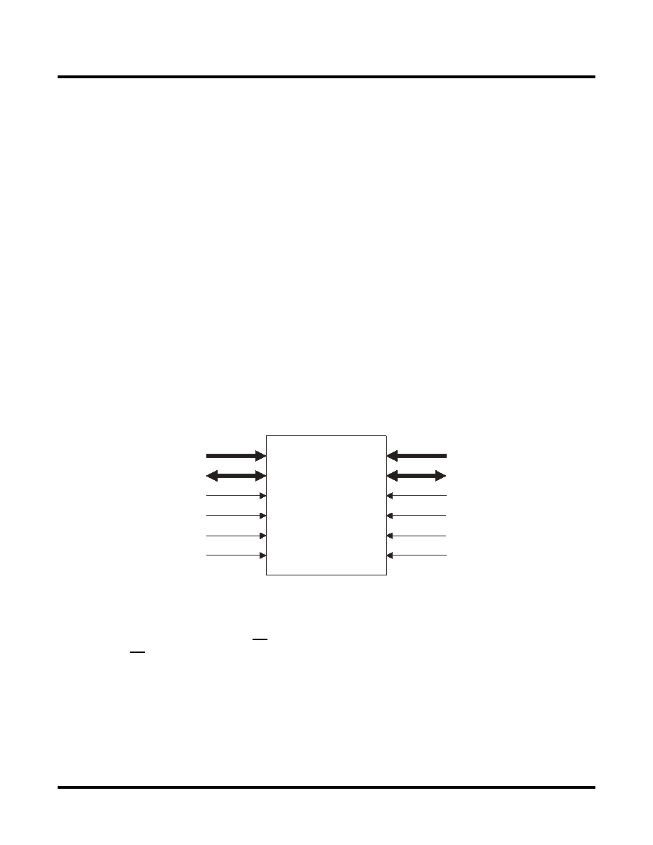
read/write clock, clock enable, write enable, and output enable. Figure 12 illustrates the sysMEM block.
The ispXPGA memory block can operate as single-port or dual-port RAM. Supported configurations are:
512 x 9 bits single-port
(8 bits data / 1 bit parity)
256 x 18 bits single-port
(16 bits data / 2 bits parity)
512 x 9 bits dual-port
(8 bits data / 1 bit parity)
256 x18 bits dual-port
(16 bits data / 2 bits parity)
The data widths of “9” and “18” are ideal for applications where parity is necessary. This allows 9 data bits, 8 data
bits plus a parity bit, 18 data bits, or 16 data bits plus two parity bits. The logic for generating and checking the par-
ity must be customized separately.
Figure 12. sysMEM Block Diagram
Read and Write Operations
The ispXPGA EBR has fully synchronous read and write operations as well as an asynchronous read operation.
These operations allow several different types of memory to be implemented in the device.
Synchronous Read: The Clock Enable (CE) and Write Enable (WE) signals control the synchronous read opera-
tion. When the CE signal is low, the clock is enabled. When the WE signal is low the read operation begins. Once
the address (ADDR) is present, a rising clock edge (or falling edge depending on polarity) causes the stored data
to be available on the DATA port. Figure 13 illustrates the synchronous read timing.
sysMEM Block
ADDRA
DATAA
WEA
OEA
CLKA
CEA
ADDRB
DATAB
WEB
OEB
CLKB
CE B
SELECT
DEVICES
DISCONTINUED
相关PDF资料 |
PDF描述 |
|---|---|
| LFX200EB-03FN256C | IC FPGA 200K GATES 256-BGA |
| HMM44DSEF | CONN EDGECARD 88POS .156 EYELET |
| HSM44DRTF | CONN EDGECARD 88POS DIP .156 SLD |
| LFECP20E-4FN672I | IC FPGA 19.7KLUTS 672FPBGA |
| HMM44DRTF | CONN EDGECARD 88POS DIP .156 SLD |
相关代理商/技术参数 |
参数描述 |
|---|---|
| LFX200EB-03F256I | 功能描述:FPGA - 现场可编程门阵列 210K Gates, 160 I/O 2.5/3.3V, -3 speed RoHS:否 制造商:Altera Corporation 系列:Cyclone V E 栅极数量: 逻辑块数量:943 内嵌式块RAM - EBR:1956 kbit 输入/输出端数量:128 最大工作频率:800 MHz 工作电源电压:1.1 V 最大工作温度:+ 70 C 安装风格:SMD/SMT 封装 / 箱体:FBGA-256 |
| LFX200EB-03F516C | 功能描述:FPGA - 现场可编程门阵列 210K 208 I/O ispJTAG RoHS:否 制造商:Altera Corporation 系列:Cyclone V E 栅极数量: 逻辑块数量:943 内嵌式块RAM - EBR:1956 kbit 输入/输出端数量:128 最大工作频率:800 MHz 工作电源电压:1.1 V 最大工作温度:+ 70 C 安装风格:SMD/SMT 封装 / 箱体:FBGA-256 |
| LFX200EB-03F516I | 功能描述:FPGA - 现场可编程门阵列 210K 208 I/O ispJTAG RoHS:否 制造商:Altera Corporation 系列:Cyclone V E 栅极数量: 逻辑块数量:943 内嵌式块RAM - EBR:1956 kbit 输入/输出端数量:128 最大工作频率:800 MHz 工作电源电压:1.1 V 最大工作温度:+ 70 C 安装风格:SMD/SMT 封装 / 箱体:FBGA-256 |
| LFX200EB-03FH516C | 功能描述:FPGA - 现场可编程门阵列 Use LFX200EB-03F516C RoHS:否 制造商:Altera Corporation 系列:Cyclone V E 栅极数量: 逻辑块数量:943 内嵌式块RAM - EBR:1956 kbit 输入/输出端数量:128 最大工作频率:800 MHz 工作电源电压:1.1 V 最大工作温度:+ 70 C 安装风格:SMD/SMT 封装 / 箱体:FBGA-256 |
| LFX200EB-03FH516I | 功能描述:FPGA - 现场可编程门阵列 Use LFX200EB-03F516I RoHS:否 制造商:Altera Corporation 系列:Cyclone V E 栅极数量: 逻辑块数量:943 内嵌式块RAM - EBR:1956 kbit 输入/输出端数量:128 最大工作频率:800 MHz 工作电源电压:1.1 V 最大工作温度:+ 70 C 安装风格:SMD/SMT 封装 / 箱体:FBGA-256 |
发布紧急采购,3分钟左右您将得到回复。