- 您现在的位置:买卖IC网 > PDF目录299403 > LFXP15C-4FN256C (LATTICE SEMICONDUCTOR CORP) PDF资料下载
参数资料
| 型号: | LFXP15C-4FN256C |
| 厂商: | LATTICE SEMICONDUCTOR CORP |
| 元件分类: | FPGA |
| 中文描述: | FPGA, 1932 CLBS, PBGA256 |
| 封装: | 17 X 17 MM, LEAD FREE, FPBGA-256 |
| 文件页数: | 36/130页 |
| 文件大小: | 1312K |
| 代理商: | LFXP15C-4FN256C |
第1页第2页第3页第4页第5页第6页第7页第8页第9页第10页第11页第12页第13页第14页第15页第16页第17页第18页第19页第20页第21页第22页第23页第24页第25页第26页第27页第28页第29页第30页第31页第32页第33页第34页第35页当前第36页第37页第38页第39页第40页第41页第42页第43页第44页第45页第46页第47页第48页第49页第50页第51页第52页第53页第54页第55页第56页第57页第58页第59页第60页第61页第62页第63页第64页第65页第66页第67页第68页第69页第70页第71页第72页第73页第74页第75页第76页第77页第78页第79页第80页第81页第82页第83页第84页第85页第86页第87页第88页第89页第90页第91页第92页第93页第94页第95页第96页第97页第98页第99页第100页第101页第102页第103页第104页第105页第106页第107页第108页第109页第110页第111页第112页第113页第114页第115页第116页第117页第118页第119页第120页第121页第122页第123页第124页第125页第126页第127页第128页第129页第130页
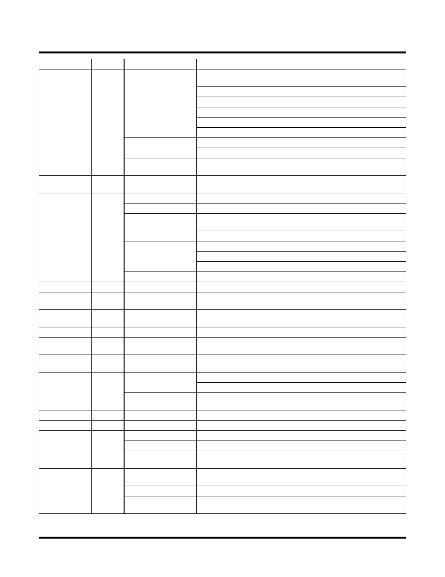
7-2
Revision History
Lattice Semiconductor
LatticeXP Family Data Sheet
September 2005
(cont.)
03.0
(cont.)
DC and Switching
Characteristics (cont.)
Updated Typical Building Block Function Performance timing numbers.
Updated External Switching Characteristics timing numbers.
Updated Internal Timing Parameters.
Updated LatticeXP Family timing adders.
Updated LatticeXP "C" Sleep Mode timing numbers.
Updated JTAG Port Timing numbers.
Pinout Information
Added clarification to SLEEPN and TOE description.
Clarification of dedicated LVDS outputs.
Supplemental
Information
Updated list of technical notes.
September 2005
03.1
Pinout Information
Power Supply and NC Connections table corrected VCCP1 pin number
for 208 PQFP.
December 2005
04.0
Introduction
Moved data sheet from Advance to Final.
Architecture
Added clarification to Typical I/O Behavior During Power-up section.
DC and Switching
Characteristics
Added clarification to Recommended Operating Conditions.
Updated timing numbers.
Pinout Information
Updated Signal Descriptions table.
Added clarification to Differential I/O Per Bank.
Updated Differential dedicated LVDS output support.
Ordering Information
Added 208 PQFP lead-free package and ordering part numbers.
February 2006
04.1
Pinout Information
Corrected description of Signal Names VREF1(x) and VREF2(x).
March 2006
04.2
DC and Switching
Characteristics
Corrected condition for IIL and IIH.
March 2006
04.3
DC and Switching
Characteristics
Added clarification to Recommended Operating Conditions for
VCCAUX.
April 2006
04.4
Pinout Information
Removed Bank designator "5" from SLEEPN/TOE ball function.
May 2006
04.5
DC and Switching
Characteristics
Added footnote 2 regarding threshold level for PROGRAMN to sysCON-
FIG Port Timing Specifications table.
June 2006
04.6
DC and Switching
Characteristics
Corrected LVDS25E Output Termination Example.
August 2006
04.7
Architecture
Added clarification to Typical I/O Behavior During Power-Up section.
Added clarification to Left and Right sysIO Buffer Pair section.
DC and Switching
Characteristics
Changes to LVDS25E Output Termination Example diagram.
December 2006
04.8
Architecture
EBR Asynchronous Reset section added.
February 2007
04.9
Architecture
Updated EBR Asynchronous Reset section.
July 2007
05.0
Introduction
Updated LatticeXP Family Selection Guide table.
Architecture
Updated Typical I/O Behavior During Power-up text section.
DC and Switching
Characteristics
Updated sysIO Single-Ended DC Electrical Characteristics table. Split
out LVCMOS 1.2 by supply voltage.
November 2007
05.1
DC and Switching
Characteristics
Added JTAG Port Timing Waveforms diagram.
Pinout Information
Added Thermal Management text section.
Supplemental
Information
Updated title list.
Date
Version
Section
Change Summary
相关PDF资料 |
PDF描述 |
|---|---|
| LFZ3508VXX | GENERAL PURPOSE INDUCTOR |
| LFZ2805HXX | GENERAL PURPOSE INDUCTOR |
| LF02004VTX | GENERAL PURPOSE INDUCTOR |
| LG3341-NE7501 | T-1 SINGLE COLOR LED, GREEN, 3 mm |
| LG3341-KNE9117 | T-1 SINGLE COLOR LED, GREEN, 3 mm |
相关代理商/技术参数 |
参数描述 |
|---|---|
| LFXP15C-4FN256I | 功能描述:FPGA - 现场可编程门阵列 15.4K LUTs 188 IO 1. 8/2.5/3.3V-4 Spd I RoHS:否 制造商:Altera Corporation 系列:Cyclone V E 栅极数量: 逻辑块数量:943 内嵌式块RAM - EBR:1956 kbit 输入/输出端数量:128 最大工作频率:800 MHz 工作电源电压:1.1 V 最大工作温度:+ 70 C 安装风格:SMD/SMT 封装 / 箱体:FBGA-256 |
| LFXP15C-4FN388C | 功能描述:FPGA - 现场可编程门阵列 15.4K LUTs 268 IO 1. 8/2.5/3.3V -4 Spd RoHS:否 制造商:Altera Corporation 系列:Cyclone V E 栅极数量: 逻辑块数量:943 内嵌式块RAM - EBR:1956 kbit 输入/输出端数量:128 最大工作频率:800 MHz 工作电源电压:1.1 V 最大工作温度:+ 70 C 安装风格:SMD/SMT 封装 / 箱体:FBGA-256 |
| LFXP15C-4FN388I | 功能描述:FPGA - 现场可编程门阵列 15.4K LUTs 268 IO 1. 8/2.5/3.3V-4 Spd I RoHS:否 制造商:Altera Corporation 系列:Cyclone V E 栅极数量: 逻辑块数量:943 内嵌式块RAM - EBR:1956 kbit 输入/输出端数量:128 最大工作频率:800 MHz 工作电源电压:1.1 V 最大工作温度:+ 70 C 安装风格:SMD/SMT 封装 / 箱体:FBGA-256 |
| LFXP15C-4FN484C | 功能描述:FPGA - 现场可编程门阵列 15.4K LUTs 1.8/2.5/3 .3V -4 Spd RoHS:否 制造商:Altera Corporation 系列:Cyclone V E 栅极数量: 逻辑块数量:943 内嵌式块RAM - EBR:1956 kbit 输入/输出端数量:128 最大工作频率:800 MHz 工作电源电压:1.1 V 最大工作温度:+ 70 C 安装风格:SMD/SMT 封装 / 箱体:FBGA-256 |
| LFXP15C-4FN484I | 功能描述:FPGA - 现场可编程门阵列 15.4K LUTs 1.8/2.5/3 .3V-4 Spd I RoHS:否 制造商:Altera Corporation 系列:Cyclone V E 栅极数量: 逻辑块数量:943 内嵌式块RAM - EBR:1956 kbit 输入/输出端数量:128 最大工作频率:800 MHz 工作电源电压:1.1 V 最大工作温度:+ 70 C 安装风格:SMD/SMT 封装 / 箱体:FBGA-256 |
发布紧急采购,3分钟左右您将得到回复。