- 您现在的位置:买卖IC网 > PDF目录299403 > LFXP15C-4FN256C (LATTICE SEMICONDUCTOR CORP) PDF资料下载
参数资料
| 型号: | LFXP15C-4FN256C |
| 厂商: | LATTICE SEMICONDUCTOR CORP |
| 元件分类: | FPGA |
| 中文描述: | FPGA, 1932 CLBS, PBGA256 |
| 封装: | 17 X 17 MM, LEAD FREE, FPBGA-256 |
| 文件页数: | 53/130页 |
| 文件大小: | 1312K |
| 代理商: | LFXP15C-4FN256C |
第1页第2页第3页第4页第5页第6页第7页第8页第9页第10页第11页第12页第13页第14页第15页第16页第17页第18页第19页第20页第21页第22页第23页第24页第25页第26页第27页第28页第29页第30页第31页第32页第33页第34页第35页第36页第37页第38页第39页第40页第41页第42页第43页第44页第45页第46页第47页第48页第49页第50页第51页第52页当前第53页第54页第55页第56页第57页第58页第59页第60页第61页第62页第63页第64页第65页第66页第67页第68页第69页第70页第71页第72页第73页第74页第75页第76页第77页第78页第79页第80页第81页第82页第83页第84页第85页第86页第87页第88页第89页第90页第91页第92页第93页第94页第95页第96页第97页第98页第99页第100页第101页第102页第103页第104页第105页第106页第107页第108页第109页第110页第111页第112页第113页第114页第115页第116页第117页第118页第119页第120页第121页第122页第123页第124页第125页第126页第127页第128页第129页第130页
2-26
Architecture
Lattice Semiconductor
LatticeXP Family Data Sheet
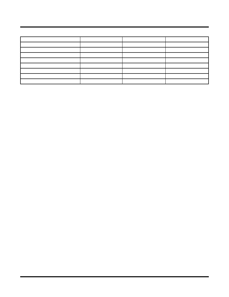
Table 2-9. Characteristics of Normal, Off and Sleep Modes
SLEEPN Pin Characteristics
The SLEEPN pin behaves as an LVCMOS input with the voltage standard appropriate to the VCC supply for the
device. This pin also has a weak pull-up typically in the order of 10A along with a Schmidt trigger and glitch filter
to prevent false triggering. An external pull-up to VCC is recommended when Sleep Mode is not used to ensure the
device stays in normal operation mode. Typically the device enters Sleep Mode several hundred ns after SLEEPN
is held at a valid low and restarts normal operation as specified in the Sleep Mode Timing table. The AC and DC
specifications portion of this data sheet show a detailed timing diagram.
Configuration and Testing
The following section describes the configuration and testing features of the LatticeXP family of devices.
IEEE 1149.1-Compliant Boundary Scan Testability
All LatticeXP devices have boundary scan cells that are accessed through an IEEE 1149.1 compliant test access
port (TAP). This allows functional testing of the circuit board, on which the device is mounted, through a serial scan
path that can access all critical logic nodes. Internal registers are linked internally, allowing test data to be shifted in
and loaded directly onto test nodes, or test data to be captured and shifted out for verification. The test access port
consists of dedicated I/Os: TDI, TDO, TCK and TMS. The test access port has its own supply voltage VCCJ and can
operate with LVCMOS3.3, 2.5, 1.8, 1.5 and 1.2 standards.
For more details on boundary scan test, please see information regarding additional technical documentation at
the end of this data sheet.
Device Configuration
All LatticeXP devices contain two possible ports that can be used for device configuration and programming. The
test access port (TAP), which supports serial configuration, and the sysCONFIG port that supports both byte-wide
and serial configuration.
The non-volatile memory in the LatticeXP can be configured in three different modes:
In sysCONFIG mode via the sysCONFIG port. Note this can also be done in background mode.
In 1532 mode via the 1149.1 port.
In background mode via the 1149.1 port. This allows the device to be operated while reprogramming takes
place.
The SRAM configuration memory can be configured in three different ways:
At power-up via the on-chip non-volatile memory.
In 1532 mode via the 1149.1 port SRAM direct configuration.
In sysCONFIG mode via the sysCONFIG port SRAM direct configuration.
Characteristic
Normal
Off
Sleep
SLEEPN Pin
High
—
Low
Static Icc
Typical <100mA
0
Typical <100uA
I/O Leakage
<10A
<1mA
<10A
Power Supplies VCC/VCCIO/VCCAUX
Normal Range
Off
Normal Range
Logic Operation
User Defined
Non Operational
Non operational
I/O Operation
User Defined
Tri-state
JTAG and Programming circuitry
Operational
Non-operational
EBR Contents and Registers
Maintained
Non-maintained
相关PDF资料 |
PDF描述 |
|---|---|
| LFZ3508VXX | GENERAL PURPOSE INDUCTOR |
| LFZ2805HXX | GENERAL PURPOSE INDUCTOR |
| LF02004VTX | GENERAL PURPOSE INDUCTOR |
| LG3341-NE7501 | T-1 SINGLE COLOR LED, GREEN, 3 mm |
| LG3341-KNE9117 | T-1 SINGLE COLOR LED, GREEN, 3 mm |
相关代理商/技术参数 |
参数描述 |
|---|---|
| LFXP15C-4FN256I | 功能描述:FPGA - 现场可编程门阵列 15.4K LUTs 188 IO 1. 8/2.5/3.3V-4 Spd I RoHS:否 制造商:Altera Corporation 系列:Cyclone V E 栅极数量: 逻辑块数量:943 内嵌式块RAM - EBR:1956 kbit 输入/输出端数量:128 最大工作频率:800 MHz 工作电源电压:1.1 V 最大工作温度:+ 70 C 安装风格:SMD/SMT 封装 / 箱体:FBGA-256 |
| LFXP15C-4FN388C | 功能描述:FPGA - 现场可编程门阵列 15.4K LUTs 268 IO 1. 8/2.5/3.3V -4 Spd RoHS:否 制造商:Altera Corporation 系列:Cyclone V E 栅极数量: 逻辑块数量:943 内嵌式块RAM - EBR:1956 kbit 输入/输出端数量:128 最大工作频率:800 MHz 工作电源电压:1.1 V 最大工作温度:+ 70 C 安装风格:SMD/SMT 封装 / 箱体:FBGA-256 |
| LFXP15C-4FN388I | 功能描述:FPGA - 现场可编程门阵列 15.4K LUTs 268 IO 1. 8/2.5/3.3V-4 Spd I RoHS:否 制造商:Altera Corporation 系列:Cyclone V E 栅极数量: 逻辑块数量:943 内嵌式块RAM - EBR:1956 kbit 输入/输出端数量:128 最大工作频率:800 MHz 工作电源电压:1.1 V 最大工作温度:+ 70 C 安装风格:SMD/SMT 封装 / 箱体:FBGA-256 |
| LFXP15C-4FN484C | 功能描述:FPGA - 现场可编程门阵列 15.4K LUTs 1.8/2.5/3 .3V -4 Spd RoHS:否 制造商:Altera Corporation 系列:Cyclone V E 栅极数量: 逻辑块数量:943 内嵌式块RAM - EBR:1956 kbit 输入/输出端数量:128 最大工作频率:800 MHz 工作电源电压:1.1 V 最大工作温度:+ 70 C 安装风格:SMD/SMT 封装 / 箱体:FBGA-256 |
| LFXP15C-4FN484I | 功能描述:FPGA - 现场可编程门阵列 15.4K LUTs 1.8/2.5/3 .3V-4 Spd I RoHS:否 制造商:Altera Corporation 系列:Cyclone V E 栅极数量: 逻辑块数量:943 内嵌式块RAM - EBR:1956 kbit 输入/输出端数量:128 最大工作频率:800 MHz 工作电源电压:1.1 V 最大工作温度:+ 70 C 安装风格:SMD/SMT 封装 / 箱体:FBGA-256 |
发布紧急采购,3分钟左右您将得到回复。