- 您现在的位置:买卖IC网 > PDF目录299403 > LFXP15C-4FN256C (LATTICE SEMICONDUCTOR CORP) PDF资料下载
参数资料
| 型号: | LFXP15C-4FN256C |
| 厂商: | LATTICE SEMICONDUCTOR CORP |
| 元件分类: | FPGA |
| 中文描述: | FPGA, 1932 CLBS, PBGA256 |
| 封装: | 17 X 17 MM, LEAD FREE, FPBGA-256 |
| 文件页数: | 50/130页 |
| 文件大小: | 1312K |
| 代理商: | LFXP15C-4FN256C |
第1页第2页第3页第4页第5页第6页第7页第8页第9页第10页第11页第12页第13页第14页第15页第16页第17页第18页第19页第20页第21页第22页第23页第24页第25页第26页第27页第28页第29页第30页第31页第32页第33页第34页第35页第36页第37页第38页第39页第40页第41页第42页第43页第44页第45页第46页第47页第48页第49页当前第50页第51页第52页第53页第54页第55页第56页第57页第58页第59页第60页第61页第62页第63页第64页第65页第66页第67页第68页第69页第70页第71页第72页第73页第74页第75页第76页第77页第78页第79页第80页第81页第82页第83页第84页第85页第86页第87页第88页第89页第90页第91页第92页第93页第94页第95页第96页第97页第98页第99页第100页第101页第102页第103页第104页第105页第106页第107页第108页第109页第110页第111页第112页第113页第114页第115页第116页第117页第118页第119页第120页第121页第122页第123页第124页第125页第126页第127页第128页第129页第130页
2-23
Architecture
Lattice Semiconductor
LatticeXP Family Data Sheet
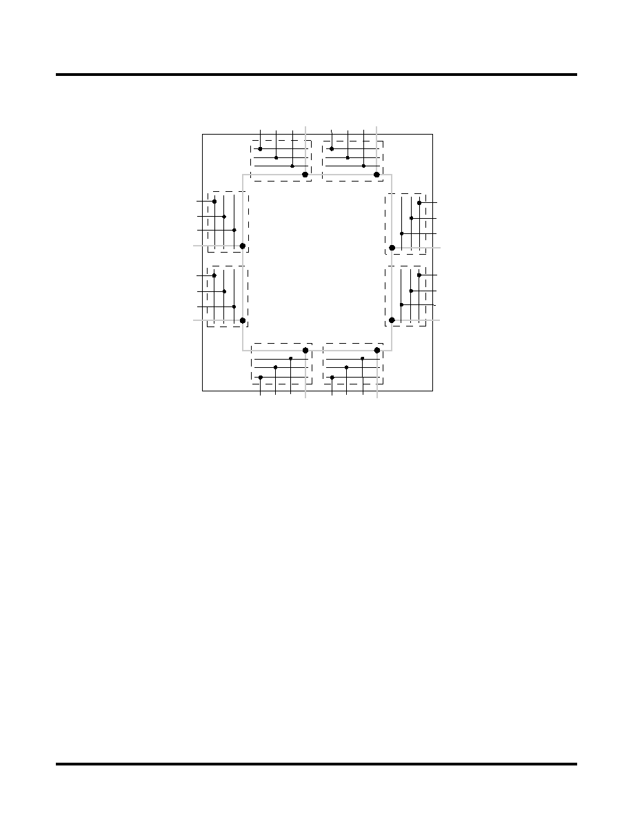
Figure 2-28. LatticeXP Banks
LatticeXP devices contain two types of sysIO buffer pairs.
1.
Top and Bottom sysIO Buffer Pair (Single-Ended Outputs Only)
The sysIO buffer pairs in the top and bottom banks of the device consist of two single-ended output drivers and
two sets of single-ended input buffers (both ratioed and referenced). The referenced input buffer can also be
configured as a differential input.
The two pads in the pair are described as “true” and “comp”, where the true pad is associated with the positive
side of the differential input buffer and the comp (complementary) pad is associated with the negative side of
the differential input buffer.
Only the I/Os on the top and bottom banks have PCI clamps. Note that the PCI clamp is enabled after VCC,
VCCAUX and VCCIO are at valid operating levels and the device has been configured.
2.
Left and Right sysIO Buffer Pair (Differential and Single-Ended Outputs)
The sysIO buffer pairs in the left and right banks of the device consist of two single-ended output drivers, two
sets of single-ended input buffers (both ratioed and referenced) and one differential output driver. The refer-
enced input buffer can also be configured as a differential input. In these banks the two pads in the pair are
described as “true” and “comp”, where the true pad is associated with the positive side of the differential I/O,
and the comp (complementary) pad is associated with the negative side of the differential I/O.
Select I/Os in the left and right banks have LVDS differential output drivers. Refer to the Logic Signal Connec-
tions tables for more information.
V
REF1(2)
GND
Bank
2
V
CCIO2
V
REF2(2)
V
REF1(3)
GND
Bank
3
V
CCIO3
V
REF2(3)
V
REF1(7)
GND
Bank
7
V
CCIO7
V
REF2(7)
V
REF1(6)
GND
Note: N and M are the maximum number of I/Os per bank.
Bank
6
V
CCIO6
V
REF2(6)
V
REF1(5)
GND
Bank 5
V
CCIO5
V
REF2(5)
V
REF1(4)
GND
Bank 4
V
CCIO4
V
REF2(4)
V
REF1(
0)
GND
Bank 0
V
CCIO0
V
REF2(
0)
V
REF1(1)
GND
Bank 1
V
CCIO1
V
REF2(1)
1
M
1
M
1
M
1
M
1N
相关PDF资料 |
PDF描述 |
|---|---|
| LFZ3508VXX | GENERAL PURPOSE INDUCTOR |
| LFZ2805HXX | GENERAL PURPOSE INDUCTOR |
| LF02004VTX | GENERAL PURPOSE INDUCTOR |
| LG3341-NE7501 | T-1 SINGLE COLOR LED, GREEN, 3 mm |
| LG3341-KNE9117 | T-1 SINGLE COLOR LED, GREEN, 3 mm |
相关代理商/技术参数 |
参数描述 |
|---|---|
| LFXP15C-4FN256I | 功能描述:FPGA - 现场可编程门阵列 15.4K LUTs 188 IO 1. 8/2.5/3.3V-4 Spd I RoHS:否 制造商:Altera Corporation 系列:Cyclone V E 栅极数量: 逻辑块数量:943 内嵌式块RAM - EBR:1956 kbit 输入/输出端数量:128 最大工作频率:800 MHz 工作电源电压:1.1 V 最大工作温度:+ 70 C 安装风格:SMD/SMT 封装 / 箱体:FBGA-256 |
| LFXP15C-4FN388C | 功能描述:FPGA - 现场可编程门阵列 15.4K LUTs 268 IO 1. 8/2.5/3.3V -4 Spd RoHS:否 制造商:Altera Corporation 系列:Cyclone V E 栅极数量: 逻辑块数量:943 内嵌式块RAM - EBR:1956 kbit 输入/输出端数量:128 最大工作频率:800 MHz 工作电源电压:1.1 V 最大工作温度:+ 70 C 安装风格:SMD/SMT 封装 / 箱体:FBGA-256 |
| LFXP15C-4FN388I | 功能描述:FPGA - 现场可编程门阵列 15.4K LUTs 268 IO 1. 8/2.5/3.3V-4 Spd I RoHS:否 制造商:Altera Corporation 系列:Cyclone V E 栅极数量: 逻辑块数量:943 内嵌式块RAM - EBR:1956 kbit 输入/输出端数量:128 最大工作频率:800 MHz 工作电源电压:1.1 V 最大工作温度:+ 70 C 安装风格:SMD/SMT 封装 / 箱体:FBGA-256 |
| LFXP15C-4FN484C | 功能描述:FPGA - 现场可编程门阵列 15.4K LUTs 1.8/2.5/3 .3V -4 Spd RoHS:否 制造商:Altera Corporation 系列:Cyclone V E 栅极数量: 逻辑块数量:943 内嵌式块RAM - EBR:1956 kbit 输入/输出端数量:128 最大工作频率:800 MHz 工作电源电压:1.1 V 最大工作温度:+ 70 C 安装风格:SMD/SMT 封装 / 箱体:FBGA-256 |
| LFXP15C-4FN484I | 功能描述:FPGA - 现场可编程门阵列 15.4K LUTs 1.8/2.5/3 .3V-4 Spd I RoHS:否 制造商:Altera Corporation 系列:Cyclone V E 栅极数量: 逻辑块数量:943 内嵌式块RAM - EBR:1956 kbit 输入/输出端数量:128 最大工作频率:800 MHz 工作电源电压:1.1 V 最大工作温度:+ 70 C 安装风格:SMD/SMT 封装 / 箱体:FBGA-256 |
发布紧急采购,3分钟左右您将得到回复。