- 您现在的位置:买卖IC网 > PDF目录180109 > M25PE40VMW6G (STMICROELECTRONICS) 512K X 8 SPI BUS SERIAL EEPROM, PDSO8 PDF资料下载
参数资料
| 型号: | M25PE40VMW6G |
| 厂商: | STMICROELECTRONICS |
| 元件分类: | PROM |
| 英文描述: | 512K X 8 SPI BUS SERIAL EEPROM, PDSO8 |
| 封装: | 0.208 INCH, ROHS COMPLIANT, PLASTIC, SOP-8 |
| 文件页数: | 2/62页 |
| 文件大小: | 565K |
| 代理商: | M25PE40VMW6G |
第1页当前第2页第3页第4页第5页第6页第7页第8页第9页第10页第11页第12页第13页第14页第15页第16页第17页第18页第19页第20页第21页第22页第23页第24页第25页第26页第27页第28页第29页第30页第31页第32页第33页第34页第35页第36页第37页第38页第39页第40页第41页第42页第43页第44页第45页第46页第47页第48页第49页第50页第51页第52页第53页第54页第55页第56页第57页第58页第59页第60页第61页第62页
SPI modes
M25PE40
3
SPI modes
These devices can be driven by a microcontroller with its SPI peripheral running in either of
the two following modes:
●
CPOL=0, CPHA=0
●
CPOL=1, CPHA=1
For these two modes, input data is latched in on the rising edge of Serial Clock (C), and
output data is available from the falling edge of Serial Clock (C).
The difference between the two modes, as shown in Figure 5, is the clock polarity when the
bus master is in Standby mode and not transferring data:
●
C remains at 0 for (CPOL=0, CPHA=0)
●
C remains at 1 for (CPOL=1, CPHA=1)
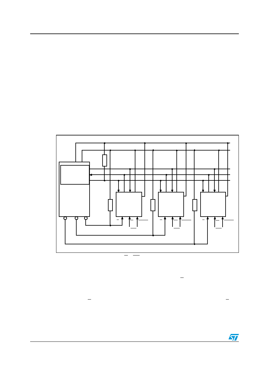
Figure 4.
Bus master and memory devices on the SPI bus
1.
The Write Protect or Top Sector Lock (W or TSL) signal should be driven, High or Low as appropriate.
Figure 4 shows an example of three devices connected to an MCU, on an SPI bus. Only one
device is selected at a time, so only one device drives the Serial Data output (Q) line at a
time, the other devices are high impedance. Resistors R (represented in Figure 4) ensure
that the M25PE40 is not selected if the Bus Master leaves the S line in the high impedance
state. As the Bus Master may enter a state where all inputs/outputs are in high impedance
at the same time (for example, when the Bus Master is reset), the clock line (C) must be
connected to an external pull-down resistor so that, when all inputs/outputs become high
impedance, the S line is pulled High while the C line is pulled Low (thus ensuring that S and
C do not become High at the same time, and so, that the tSHCH requirement is met). The
typical value of R is 100 k
, assuming that the time constant R*C
p (Cp = parasitic
capacitance of the bus line) is shorter than the time during which the Bus Master leaves the
SPI bus in high impedance.
AI13558b
SPI Bus Master
SPI memory
device
SDO
SDI
SCK
CQD
S
SPI memory
device
CQD
S
SPI memory
device
CQD
S
CS3
CS2 CS1
SPI interface with
(CPOL, CPHA) =
(0, 0) or (1, 1)
W
or
TSL
Reset
W
or
TSL
Reset
W
or
TSL
Reset
RR
R
VCC
VSS
R
相关PDF资料 |
PDF描述 |
|---|---|
| M27C1024-10F1X | 1 Mbit 64Kb x16 UV EPROM and OTP EPROM |
| M27C1024-10F3TR | 1 Mbit 64Kb x16 UV EPROM and OTP EPROM |
| M27C1024-10F3X | 1 Mbit 64Kb x16 UV EPROM and OTP EPROM |
| M27C1024-10F6TR | 1 Mbit 64Kb x16 UV EPROM and OTP EPROM |
| M27C1024-10F6X | 1 Mbit 64Kb x16 UV EPROM and OTP EPROM |
相关代理商/技术参数 |
参数描述 |
|---|---|
| M25PE40-VMW6G | 功能描述:闪存 4 Mbit Lo Vltg Page Erasable Seral 闪存 RoHS:否 制造商:ON Semiconductor 数据总线宽度:1 bit 存储类型:Flash 存储容量:2 MB 结构:256 K x 8 定时类型: 接口类型:SPI 访问时间: 电源电压-最大:3.6 V 电源电压-最小:2.3 V 最大工作电流:15 mA 工作温度:- 40 C to + 85 C 安装风格:SMD/SMT 封装 / 箱体: 封装:Reel |
| M25PE40-VMW6G_NUD | 制造商:Micron Technology Inc 功能描述: |
| M25PE40VMW6P | 制造商:STMICROELECTRONICS 制造商全称:STMicroelectronics 功能描述:4 Mbit, low voltage, Page-Erasable Serial Flash memory with byte alterability, 50 MHz SPI bus, standard pinout |
| M25PE40-VMW6P | 制造商:NUMONYX 制造商全称:Numonyx B.V 功能描述:4 Mbit, page-erasable serial Flash memory with byte alterability, 75 MHz SPI bus, standard pinout |
| M25PE40VMW6TG | 制造商:STMICROELECTRONICS 制造商全称:STMicroelectronics 功能描述:4 Mbit, low voltage, Page-Erasable Serial Flash memory with byte alterability, 50 MHz SPI bus, standard pinout |
发布紧急采购,3分钟左右您将得到回复。