- 您现在的位置:买卖IC网 > PDF目录180109 > M25PE40VMW6G (STMICROELECTRONICS) 512K X 8 SPI BUS SERIAL EEPROM, PDSO8 PDF资料下载
参数资料
| 型号: | M25PE40VMW6G |
| 厂商: | STMICROELECTRONICS |
| 元件分类: | PROM |
| 英文描述: | 512K X 8 SPI BUS SERIAL EEPROM, PDSO8 |
| 封装: | 0.208 INCH, ROHS COMPLIANT, PLASTIC, SOP-8 |
| 文件页数: | 24/62页 |
| 文件大小: | 565K |
| 代理商: | M25PE40VMW6G |
第1页第2页第3页第4页第5页第6页第7页第8页第9页第10页第11页第12页第13页第14页第15页第16页第17页第18页第19页第20页第21页第22页第23页当前第24页第25页第26页第27页第28页第29页第30页第31页第32页第33页第34页第35页第36页第37页第38页第39页第40页第41页第42页第43页第44页第45页第46页第47页第48页第49页第50页第51页第52页第53页第54页第55页第56页第57页第58页第59页第60页第61页第62页
Instructions
M25PE40
6.8
Read Lock Register (RDLR)
Note:
The Read Lock Register (RDLR) instruction is decoded only in the M25PE40 in the T9HX
process (see Important note on page 6).
The device is first selected by driving Chip Select (S) Low. The instruction code for the Read
Lock Register (RDLR) instruction is followed by a 3-byte address (A23-A0) pointing to any
location inside the concerned sector (or subsector). Each address bit is latched-in during
the rising edge of Serial Clock (C). Then the value of the Lock Register is shifted out on
Serial Data output (Q), each bit being shifted out, at a maximum frequency fC, during the
falling edge of Serial Clock (C).
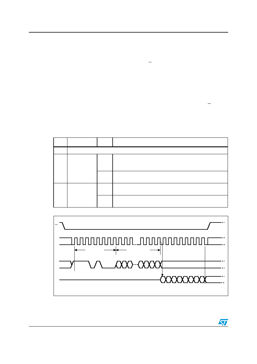
The instruction sequence is shown in Figure 14.
The Read Lock Register (RDLR) instruction is terminated by driving Chip Select (S) High at
any time during data output.
Any Read Lock Register (RDLR) instruction, while an Erase, Program or Write cycle is in
progress, is rejected without having any effects on the cycle that is in progress.
Figure 14.
Read Lock Register (RDLR) instruction sequence and data-out sequence
Table 9.
Lock Registers
Bit
Bit name
Value
Function
b7-b4
Reserved
b1
Sector Lock
Down
‘1’
The Write Lock and Lock Down bits cannot be changed. Once a
‘1’ is written to the Lock Down bit it cannot be cleared to ‘0’,
except by a reset or power-up.
‘0’
The Write Lock and Lock Down bits can be changed by writing
new values to them (default value).
b0
Sector Write
Lock
‘1’
Write, Program and Erase operations in this sector will not be
executed. The memory contents will not be changed.
‘0’
Write, Program and Erase operations in this sector are executed
and will modify the sector contents (default value).
C
D
AI10783
S
Q
23
2
1
3456789 10
28 29 30 31 32 33 34 35
22 21
3210
36 37 38
76543
1
0
High Impedance
Lock Register Out
Instruction
24-bit address
0
MSB
2
39
相关PDF资料 |
PDF描述 |
|---|---|
| M27C1024-10F1X | 1 Mbit 64Kb x16 UV EPROM and OTP EPROM |
| M27C1024-10F3TR | 1 Mbit 64Kb x16 UV EPROM and OTP EPROM |
| M27C1024-10F3X | 1 Mbit 64Kb x16 UV EPROM and OTP EPROM |
| M27C1024-10F6TR | 1 Mbit 64Kb x16 UV EPROM and OTP EPROM |
| M27C1024-10F6X | 1 Mbit 64Kb x16 UV EPROM and OTP EPROM |
相关代理商/技术参数 |
参数描述 |
|---|---|
| M25PE40-VMW6G | 功能描述:闪存 4 Mbit Lo Vltg Page Erasable Seral 闪存 RoHS:否 制造商:ON Semiconductor 数据总线宽度:1 bit 存储类型:Flash 存储容量:2 MB 结构:256 K x 8 定时类型: 接口类型:SPI 访问时间: 电源电压-最大:3.6 V 电源电压-最小:2.3 V 最大工作电流:15 mA 工作温度:- 40 C to + 85 C 安装风格:SMD/SMT 封装 / 箱体: 封装:Reel |
| M25PE40-VMW6G_NUD | 制造商:Micron Technology Inc 功能描述: |
| M25PE40VMW6P | 制造商:STMICROELECTRONICS 制造商全称:STMicroelectronics 功能描述:4 Mbit, low voltage, Page-Erasable Serial Flash memory with byte alterability, 50 MHz SPI bus, standard pinout |
| M25PE40-VMW6P | 制造商:NUMONYX 制造商全称:Numonyx B.V 功能描述:4 Mbit, page-erasable serial Flash memory with byte alterability, 75 MHz SPI bus, standard pinout |
| M25PE40VMW6TG | 制造商:STMICROELECTRONICS 制造商全称:STMicroelectronics 功能描述:4 Mbit, low voltage, Page-Erasable Serial Flash memory with byte alterability, 50 MHz SPI bus, standard pinout |
发布紧急采购,3分钟左右您将得到回复。