- 您现在的位置:买卖IC网 > PDF目录359020 > M295V100-T70XM3R (意法半导体) 1 Mbit 128Kb x8 or 64Kb x16, Boot Block Single Supply Flash Memory PDF资料下载
参数资料
| 型号: | M295V100-T70XM3R |
| 厂商: | 意法半导体 |
| 元件分类: | FLASH |
| 英文描述: | 1 Mbit 128Kb x8 or 64Kb x16, Boot Block Single Supply Flash Memory |
| 中文描述: | 1兆位的128KBx8或64Kbx16,有启动区域的单电源闪存 |
| 文件页数: | 11/30页 |
| 文件大小: | 207K |
| 代理商: | M295V100-T70XM3R |
第1页第2页第3页第4页第5页第6页第7页第8页第9页第10页当前第11页第12页第13页第14页第15页第16页第17页第18页第19页第20页第21页第22页第23页第24页第25页第26页第27页第28页第29页第30页
Toggle Bit (DQ2).
This toggle bit, together with
DQ6, can be used to determine the device status
duringthe Eraseoperations.It can alsobe usedto
identify the block being erased. During Erase or
Erase Suspend a read from a block being erased
will cause DQ2 to toggle. A read from a block not
being erased will set DQ2 to ’1’ during erase and
to DQ2 during Erase Suspend.During Chip Erase
a read operation will cause DQ2 to toggle as all
blocks are being erased. DQ2 will be set to ’1’
duringprogramoperationand whenerase is com-
plete. After erase completion and if the error bit
DQ5 is set to ’1’, DQ2 will toggle if the faulty block
is addressed.
Error Bit (DQ5).
This bit is set to ’1’ by the P/E.C.
when there is a failure of programming, block
erase, or chip erase that results in invalid data in
thememoryblock.In caseof anerrorinblockerase
or program,the blockin whichtheerror occuredor
to which the programmed data belongs, must be
discarded. The DQ5 failure condition will also ap-
pearifa usertriesto programa’1’toa locationthat
is previouslyprogrammedto ’0’. OtherBlocksmay
stillbe used.TheerrorbitresetsafteraRead/Reset
(RD)instruction. In caseof successof Program or
Erase, the error bit will be set to ’0’.
EraseTimer Bit (DQ3).
This bit is setto ’0’ by the
P/E.C. when the last block Erase command has
been entered to the Command Interface and it is
awaiting the Erase start. When the erase timeout
periodis finished,after80
μ
s to120
μ
s,DQ3returns
to ’1’.
Coded Cycles
The two Coded cyclesunlockthe CommandInter-
face.They are followedby an input commandor a
confirmationcommand.The Codedcycles consist
of writing the data AAh at address AAAAh in the
Byte-wide configuration and at address 5555h in
the Word-wide configuration during the first cycle.
During the secondcycle the Coded cycles consist
of writing the data 55h at address 5555h in the
Byte-wide configuration and at address 2AAAh in
theWord-wideconfiguration.In the Byte-widecon-
figurationtheaddresslinesA–1to A14are valid,in
Word-wideA0 to A14arevalid,otheraddresslines
are’don’t care’. The Coded cycles happenon first
andsecondcycles of thecommandwrite or on the
fourthand fifth cycles.
Instructions
SeeTable 8.
Read/Reset (RD) Instruction.
The Read/Reset
instruction consists of one write cycle giving the
commandF0h.Itcanbeoptionallyprecededby the
twoCodedcycles.Subsequentreadoperationswill
read the memory array addressed and output the
data read. A wait state of 10
μ
s is necessary after
Read/Reset prior to any valid read if the memory
was in an Erase mode when the RD instruction is
given.
Auto Select (AS) Instruction.
This instruction
uses the two Coded cycles followed by one write
cycle giving the command90h to address AAAAh
in the Byte-wide configurationor address5555hin
the Word-wide configuration for command set-up.
A subsequent read will output the manufacturer
code and the device code or the block protection
status dependingon the levels of A0 and A1. The
manufacturer code, 20h, is output when the ad-
dresseslinesA0 and A1are Low,the devicecode,
D0h for Top Boot, D1h for Bottom Boot is output
whenA0 isHigh with A1 Low.
The AS instruction also allowsaccess to the block
protectionstatus.After givingtheASinstruction,A0
is set to V
IL
with A1 at V
IH
, while A12-A15 define
the address of the block to be verified. A read in
these conditions will output a 01h if the block is
protectedand a 00h if the blockis not protected.
Program (PG) Instruction.
This instruction uses
four write cycles. Both for Byte-wide configuration
and for Word-wide configuration. The Program
command A0h is written to addressAAAAh in the
Byte-wideconfigurationortoaddress5555h inthe
Word-wideconfigurationonthethirdcycleaftertwo
Codedcycles. Afourthwrite operationlatchesthe
Addresson thefallingedge of W orE and theData
to be written on the rising edge and starts the
P/E.C.Readoperationsoutputthe StatusRegister
bits after the programming has started. Memory
programmingis madeonlyby writing ’0’in placeof
’1’.StatusbitsDQ6andDQ7determineif program-
mingison-goingandDQ5allowsverificationof any
possible error. Programming at an address not in
blocks being erased is also possible during erase
suspend. In this case, DQ2 will toggle at the ad-
dressbeing programmed.
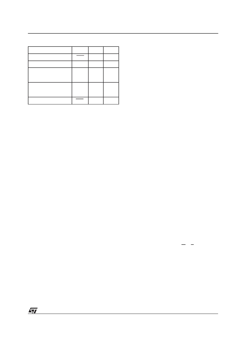
Mode
DQ7
DQ6
DQ2
Program
DQ7
Toggle
1
Erase
0
Toggle
Note 1
Erase Suspend Read
(in EraseSuspend
block)
1
1
Toggle
Erase Suspend Read
(outside Erase Suspend
block)
DQ7
DQ6
DQ2
Erase Suspend Program
DQ7
Toggle
N/A
Note:
1. Toggle if the address is within a block being erased.
’1’ if the address is within a block not being erased.
Table10. Pollingand Toggle Bits
11/30
M29F100T, M29F100B
相关PDF资料 |
PDF描述 |
|---|---|
| M295V100B-T45N6T | 8-Bit, 0.1 us MDAC, Parallel Input, Fast Control Signalling for DSP, Easy Micro Interface 16-TSSOP -25 to 85 |
| M295V200T-55M1R | CONNECTOR ACCESSORY |
| M295V400T-55N6R | 4 Mbit 512Kb x8 or 256Kb x16, Boot Block Single Supply Flash Memory |
| M295V800AB90M1T | Circular Connector; No. of Contacts:37; Series:JT02R; Body Material:Aluminum; Connecting Termination:Crimp; Connector Shell Size:14; Circular Contact Gender:Socket; Circular Shell Style:Box Mount Receptacle; Insert Arrangement:14-35 |
| M29DW128F60NF1 | 128 Mbit (16Mb x8 or 8Mb x16, Multiple Bank, Page, Boot Block) 3V Supply, Flash Memory |
相关代理商/技术参数 |
参数描述 |
|---|---|
| M295V100-T70XM3TR | 制造商:STMICROELECTRONICS 制造商全称:STMicroelectronics 功能描述:1 Mbit 128Kb x8 or 64Kb x16, Boot Block Single Supply Flash Memory |
| M295V100-T70XM6R | 制造商:STMICROELECTRONICS 制造商全称:STMicroelectronics 功能描述:1 Mbit 128Kb x8 or 64Kb x16, Boot Block Single Supply Flash Memory |
| M295V100-T70XM6TR | 制造商:STMICROELECTRONICS 制造商全称:STMicroelectronics 功能描述:1 Mbit 128Kb x8 or 64Kb x16, Boot Block Single Supply Flash Memory |
| M295V100-T70XN1R | 制造商:STMICROELECTRONICS 制造商全称:STMicroelectronics 功能描述:1 Mbit 128Kb x8 or 64Kb x16, Boot Block Single Supply Flash Memory |
| M295V100-T70XN1TR | 制造商:STMICROELECTRONICS 制造商全称:STMicroelectronics 功能描述:1 Mbit 128Kb x8 or 64Kb x16, Boot Block Single Supply Flash Memory |
发布紧急采购,3分钟左右您将得到回复。