- 您现在的位置:买卖IC网 > PDF目录359020 > M295V100-T70XM3R (意法半导体) 1 Mbit 128Kb x8 or 64Kb x16, Boot Block Single Supply Flash Memory PDF资料下载
参数资料
| 型号: | M295V100-T70XM3R |
| 厂商: | 意法半导体 |
| 元件分类: | FLASH |
| 英文描述: | 1 Mbit 128Kb x8 or 64Kb x16, Boot Block Single Supply Flash Memory |
| 中文描述: | 1兆位的128KBx8或64Kbx16,有启动区域的单电源闪存 |
| 文件页数: | 8/30页 |
| 文件大小: | 207K |
| 代理商: | M295V100-T70XM3R |
第1页第2页第3页第4页第5页第6页第7页当前第8页第9页第10页第11页第12页第13页第14页第15页第16页第17页第18页第19页第20页第21页第22页第23页第24页第25页第26页第27页第28页第29页第30页
Block Temporary Unprotection.
Any previously
protectedblock can be temporarily unprotectedin
ordertochangestoreddata.Thetemporaryunpro-
tection mode is activated by bringing RP to V
ID
.
During the temporary unprotection mode the pre-
viously protected blocks are unprotected. A block
can be selected and data can be modified by
executingtheEraseorPrograminstructionwiththe
RPsignal held at V
ID
. When RPis returnedto V
IH
,
all the previously protected blocks are again pro-
tected.
Block Unprotection.
All protected blocks can be
unprotected on programming equipment to allow
updating of bit contents. All blocks must first be
protectedbeforethe unprotectionoperation.Block
unprotectionis activatedwhen A9, G and E are at
V
ID
and A12, A15 at V
IH
. The Block Unprotection
algorithm is shown in Figure 15. Unprotection is
initiatedby theedgeofWfallingto V
IL
.Aftera delay
of 10ms, the unprotection operation will end. Un-
protectionverifyis achievedbybringingGand Eto
V
IL
whileA0 is at V
IL
, A6 andA1 are at V
IH
andA9
remains at V
ID
. In these conditions, reading the
outputdata willyield 00hif theblockdefinedby the
inputsA12-A15has been succesfullyunprotected.
Eachblock mustbeseparatelyverified bygivingits
address in order to ensure that it has beenunpro-
tected.
INSTRUCTIONS AND COMMANDS
The Command Interface latches commands writ-
ten to the memory. Instructionsare made up from
one or more commands to perform Read Memory
Array,ReadElectronicSignature,ReadBlockPro-
tection, Program, Block Erase, Chip Erase, Erase
Suspend and Erase Resume. Commands are
made of
address and data sequences. The in-
structionsrequirefrom 1 to6 cycles,thefirst or first
threeof whichare alwayswrite operationsusedto
initiate the instruction. They are followed by either
furtherwritecycles toconfirmthe first commandor
executethecommandimmediately. Commandse-
quencing must be followed exactly. Any invalid
combinationof commands will reset the device to
Read Array. The increased number of cycles has
been chosen to assure maximum data security.
Instructions are initialised by two initial Coded cy-
cleswhichunlockthe CommandInterface.In addi-
tion, for Erase, instruction confirmation is again
precededby the twoCoded cycles.
Status RegisterBits
P/E.C.statusis indicatedduringexecutionbyData
Polling on DQ7, detection of Toggle on DQ6 and
DQ2, or Error on DQ5 and Erase Timer DQ3 bits.
Any read attempt during Program or Erase com-
mandexecutionwill automaticallyoutputthesefive
StatusRegisterbits.The P/E.C.automaticallysets
bits DQ2, DQ3, DQ5, DQ6 and DQ7. Other bits
(DQ0, DQ1 and DQ4) are reserved for future use
and should be masked. See Tables9 and 10.
Data Polling Bit (DQ7).
When Programming op-
erations are in progress, this bit outputs the com-
plement of the bit being programmed on DQ7.
DuringErase operation,it outputsa ’0’.After com-
pletionof the operation,DQ7will outputthe bit last
programmedor a ’1’ after erasing. Data Polling is
valid and only effective during P/E.C. operation,
that is after the fourthW pulse for programmingor
after the sixth W pulse for erase. It must be per-
formedat theaddress being programmedor at an
address within the block being erased. If all the
blocksselectedfor erasureare protected,DQ7will
be setto ’0’for about100
μ
s, andthenreturn to the
previous addressed memory data value. See Fig-
ure11for the Data Pollingflowchartand Figure10
for the Data Polling waveforms. DQ7 will also flag
the Erase Suspend mode by switching from ’0’ to
’1’ at the start of the Erase Suspend. In order to
monitor DQ7 in the Erase Suspend mode an ad-
dress within a block being erased must be pro-
vided. For a Read Operation in Erase Suspend
mode, DQ7 will output ’1’ if the read is attempted
onablockbeingerasedandthedatavalueon other
blocks. During Program operation in Erase Sus-
pend Mode, DQ7 will have the samebehaviour as
in the normal program execution outside of the
suspendmode.
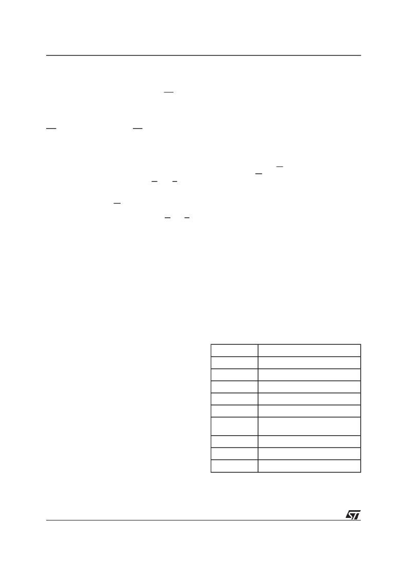
Hex Code
Command
00h
Invalid/Reserved
10h
Chip Erase Confirm
20h
Reserved
30h
Block Erase Resume/Confirm
80h
Set-up Erase
90h
Read Electronic Signature/
Block Protection Status
A0h
Program
B0h
Erase Suspend
F0h
Read Array/Reset
Table 7. Commands
8/30
M29F100T, M29F100B
相关PDF资料 |
PDF描述 |
|---|---|
| M295V100B-T45N6T | 8-Bit, 0.1 us MDAC, Parallel Input, Fast Control Signalling for DSP, Easy Micro Interface 16-TSSOP -25 to 85 |
| M295V200T-55M1R | CONNECTOR ACCESSORY |
| M295V400T-55N6R | 4 Mbit 512Kb x8 or 256Kb x16, Boot Block Single Supply Flash Memory |
| M295V800AB90M1T | Circular Connector; No. of Contacts:37; Series:JT02R; Body Material:Aluminum; Connecting Termination:Crimp; Connector Shell Size:14; Circular Contact Gender:Socket; Circular Shell Style:Box Mount Receptacle; Insert Arrangement:14-35 |
| M29DW128F60NF1 | 128 Mbit (16Mb x8 or 8Mb x16, Multiple Bank, Page, Boot Block) 3V Supply, Flash Memory |
相关代理商/技术参数 |
参数描述 |
|---|---|
| M295V100-T70XM3TR | 制造商:STMICROELECTRONICS 制造商全称:STMicroelectronics 功能描述:1 Mbit 128Kb x8 or 64Kb x16, Boot Block Single Supply Flash Memory |
| M295V100-T70XM6R | 制造商:STMICROELECTRONICS 制造商全称:STMicroelectronics 功能描述:1 Mbit 128Kb x8 or 64Kb x16, Boot Block Single Supply Flash Memory |
| M295V100-T70XM6TR | 制造商:STMICROELECTRONICS 制造商全称:STMicroelectronics 功能描述:1 Mbit 128Kb x8 or 64Kb x16, Boot Block Single Supply Flash Memory |
| M295V100-T70XN1R | 制造商:STMICROELECTRONICS 制造商全称:STMicroelectronics 功能描述:1 Mbit 128Kb x8 or 64Kb x16, Boot Block Single Supply Flash Memory |
| M295V100-T70XN1TR | 制造商:STMICROELECTRONICS 制造商全称:STMicroelectronics 功能描述:1 Mbit 128Kb x8 or 64Kb x16, Boot Block Single Supply Flash Memory |
发布紧急采购,3分钟左右您将得到回复。