- 您现在的位置:买卖IC网 > PDF目录80495 > MC68302CRC16C (MOTOROLA INC) 4 CHANNEL(S), 10M bps, LOCAL AREA NETWORK CONTROLLER, CPGA132 PDF资料下载
参数资料
| 型号: | MC68302CRC16C |
| 厂商: | MOTOROLA INC |
| 元件分类: | 微控制器/微处理器 |
| 英文描述: | 4 CHANNEL(S), 10M bps, LOCAL AREA NETWORK CONTROLLER, CPGA132 |
| 封装: | PGA-132 |
| 文件页数: | 55/128页 |
| 文件大小: | 641K |
| 代理商: | MC68302CRC16C |
第1页第2页第3页第4页第5页第6页第7页第8页第9页第10页第11页第12页第13页第14页第15页第16页第17页第18页第19页第20页第21页第22页第23页第24页第25页第26页第27页第28页第29页第30页第31页第32页第33页第34页第35页第36页第37页第38页第39页第40页第41页第42页第43页第44页第45页第46页第47页第48页第49页第50页第51页第52页第53页第54页当前第55页第56页第57页第58页第59页第60页第61页第62页第63页第64页第65页第66页第67页第68页第69页第70页第71页第72页第73页第74页第75页第76页第77页第78页第79页第80页第81页第82页第83页第84页第85页第86页第87页第88页第89页第90页第91页第92页第93页第94页第95页第96页第97页第98页第99页第100页第101页第102页第103页第104页第105页第106页第107页第108页第109页第110页第111页第112页第113页第114页第115页第116页第117页第118页第119页第120页第121页第122页第123页第124页第125页第126页第127页第128页
MOTOROLA
MC68EN302 REFERENCE MANUAL
3-1
SECTION 3
MC68EN302 DRAM CONTROL MODULE
3.1 INTRODUCTION
The MC68EN302, like its predecessor the MC68302, can be connected with DRAM-type
memories easily. The difference in the MC68EN302 lies in the DRAM Control Module
(DCM), which was developed to provide seamless integration of the 68000 core with DRAM
memories. The MC68EN302 DRAM controller is able to support up to two 16-bit wide banks
and an address range from 128kbytes to 8Mbytes. Selection between the two banks occurs
externally through the MC68EN302 RAS1–RAS0 signals, and byte selection occurs via the
CAS1–CAS0 signals. The user is able to select cycle lengths ranging in duration from 4 to
7 clocks. The MC68EN302 also provides programmable refresh rates which can range
anywhere from 16 to 4096 system clocks, or be disabled altogether.
3.2 MEMORY MAP
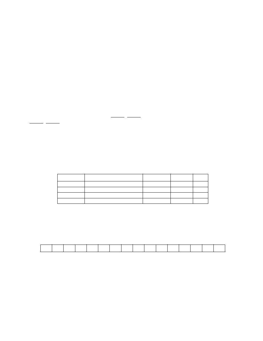
Table 3-1 shows the basic memory map of the DRAM Control Module registers.
3.3 DRAM CONFIGURATION REGISTER (DCR)
This register controls the specific operation of each bank of DRAM and is initialized to zero
at hardware reset.
Bits 15–12—Reserved. Should be written to zero by the host processor. These bits are
always read as zero.
E1-E0—Refresh Enable Bits.
0 = Disable refresh operation in the corresponding DRAM bank
1 = Enable refresh operation in the corresponding bank.
Table 3-1. DRAM Controller Registers
ADDRESS
NAME
MNEMONIC
TYPE
FC
MOBA + 010
DRAM Configuration Register
DCR
Read/Write
S
MOBA + 012
DRAM Refresh Register
DRFRSH
Read/Write
S
MOBA + 014
DRAM Bank 0 Base Address Register
DBA0
Read/Write
S
MOBA + 016
DRAM Bank 1 Base Address Register
DBA1
Read/Write
S
15
14
13
12
11
10
9876543210
0000
E1
E0
PE1
PE0
P1
P0
W1
W0
WP1
WP0
S/U1
S/U0
相关PDF资料 |
PDF描述 |
|---|---|
| MC9S12DJ256CVFU | 16-BIT, FLASH, 25 MHz, MICROCONTROLLER, PQFP80 |
| MC68HC705C5CP | 8-BIT, OTPROM, 2.1 MHz, MICROCONTROLLER, PDIP40 |
| M37471M8-XXXSP | 8-BIT, MROM, 8 MHz, MICROCONTROLLER, PDIP42 |
| M37478M4-XXXSP | 8-BIT, MROM, 8 MHz, MICROCONTROLLER, PDIP42 |
| M37478M8-XXXFP | 8-BIT, MROM, 8 MHz, MICROCONTROLLER, PQFP56 |
相关代理商/技术参数 |
参数描述 |
|---|---|
| MC68302CRC20 | 制造商:MOTOROLA 制造商全称:Motorola, Inc 功能描述:Integrated Multiprotocol Processor User’s Manual |
| MC68302CRC20C | 功能描述:微处理器 - MPU 68K INTGR COM PROC DMA RoHS:否 制造商:Atmel 处理器系列:SAMA5D31 核心:ARM Cortex A5 数据总线宽度:32 bit 最大时钟频率:536 MHz 程序存储器大小:32 KB 数据 RAM 大小:128 KB 接口类型:CAN, Ethernet, LIN, SPI,TWI, UART, USB 工作电源电压:1.8 V to 3.3 V 最大工作温度:+ 85 C 安装风格:SMD/SMT 封装 / 箱体:FBGA-324 |
| MC68302EH16C | 功能描述:微处理器 - MPU 68K INTGR COM PROC DMA RoHS:否 制造商:Atmel 处理器系列:SAMA5D31 核心:ARM Cortex A5 数据总线宽度:32 bit 最大时钟频率:536 MHz 程序存储器大小:32 KB 数据 RAM 大小:128 KB 接口类型:CAN, Ethernet, LIN, SPI,TWI, UART, USB 工作电源电压:1.8 V to 3.3 V 最大工作温度:+ 85 C 安装风格:SMD/SMT 封装 / 箱体:FBGA-324 |
| MC68302EH16C | 制造商:Freescale Semiconductor 功能描述:32-Bit Microcontroller IC |
| MC68302EH16CB1 | 功能描述:微处理器 - MPU 68K INTGR COM PROC DMA RoHS:否 制造商:Atmel 处理器系列:SAMA5D31 核心:ARM Cortex A5 数据总线宽度:32 bit 最大时钟频率:536 MHz 程序存储器大小:32 KB 数据 RAM 大小:128 KB 接口类型:CAN, Ethernet, LIN, SPI,TWI, UART, USB 工作电源电压:1.8 V to 3.3 V 最大工作温度:+ 85 C 安装风格:SMD/SMT 封装 / 箱体:FBGA-324 |
发布紧急采购,3分钟左右您将得到回复。