- 您现在的位置:买卖IC网 > Datasheet目录476 > MCP2030A-I/P (Microchip Technology)IC KEYLESS ENTRY AFE 3CH 14PDIP Datasheet资料下载
参数资料
| 型号: | MCP2030A-I/P |
| 厂商: | Microchip Technology |
| 文件页数: | 44/66页 |
| 文件大小: | 0K |
| 描述: | IC KEYLESS ENTRY AFE 3CH 14PDIP |
| 标准包装: | 30 |
| RF 型: | PEG,TPMS |
| 频率: | 125kHz |
| 特点: | 4 通道 |
| 封装/外壳: | 14-DIP(0.300",7.62mm) |
| 供应商设备封装: | 14-PDIP |
| 包装: | 管件 |
第1页第2页第3页第4页第5页第6页第7页第8页第9页第10页第11页第12页第13页第14页第15页第16页第17页第18页第19页第20页第21页第22页第23页第24页第25页第26页第27页第28页第29页第30页第31页第32页第33页第34页第35页第36页第37页第38页第39页第40页第41页第42页第43页当前第44页第45页第46页第47页第48页第49页第50页第51页第52页第53页第54页第55页第56页第57页第58页第59页第60页第61页第62页第63页第64页第65页第66页
�� �
�
�MCP2030�
�5.30.2�
�CARRIER� CLOCK� OUTPUT�
�When� the� device� receives� an� SPI� command� during� the�
�When� the� carrier� clock� output� is� selected,� the� LFDATA�
�output� is� a� square� pulse� of� the� input� carrier� clock� and�
�available� as� soon� as� the� AGC� stabilization� time� (T� AGC� )�
�is� completed.� There� are� two� Configuration� register�
�options� for� the� carrier� clock� output:� (a)� clock� divide-by�
�one� or� (b)� clock� divide-by� four,� depending� on� bit�
�DATOUT<7>� of� Configuration� Register� 2� (Register� 5-�
�3).� The� carrier� clock� output� is� available� immediately�
�after� the� AGC� settling� time.� The� Output� Enable� Filter,�
�AGCSIG,� and� MODMIN� options� are� applicable� for� the�
�carrier� clock� output� in� the� same� way� as� the� demodu-�
�lated� output.� The� input� channel� can� be� individually�
�enabled� or� disabled� for� the� output.� If� more� than� one�
�channel� is� enabled,� the� output� is� the� sum� of� each� out-�
�put� of� all� enabled� channels.� Therefore,� the� carrier� clock�
�output� waveform� is� not� as� precise� as� when� only� one�
�channel� is� enabled.� It� is� recommended� to� enable� one�
�channel� only� if� a� precise� output� waveform� is� desired.�
�There� will� be� no� valid� output� if� all� three� channels� are�
�disabled.� See� Figure� 2-32� for� carrier� clock� output�
�examples.�
�Related� Configuration� register� bits� :�
�?� Configuration� Register� 1� (Register� 5-2),�
�RSSI� output,� the� RSSI� mode� is� temporary� disabled�
�until� the� SPI� communication� is� completed.� It� returns� to�
�the� RSSI� mode� again� after� the� SPI� communication� is�
�completed.� The� RSSI� mode� is� held� until� another�
�output� type� is� selected� (CS� low� turns� off� the� RSSI�
�signal).� To� obtain� the� RSSI� output� for� a� particular� input�
�channel,� or� to� save� operating� power,� the� input� channel�
�can� be� individually� enabled� or� disabled.� If� more� than�
�one� channel� is� enabled,� the� RSSI� output� is� from� the�
�strongest� signal� channel.� There� will� be� no� valid� output�
�if� all� three� channels� are� disabled.�
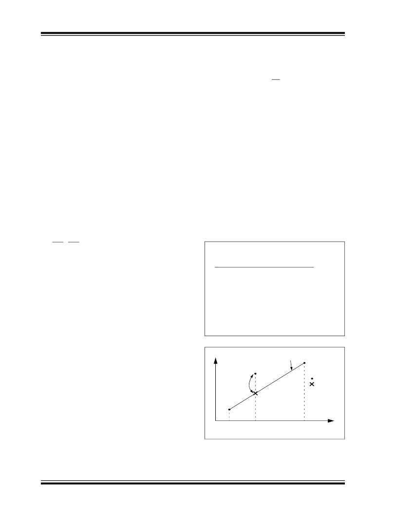
�The� RSSI� output� current� is� linearly� proportional� to� the�
�input� signal� strength.� There� are� variations� between�
�channel� to� channel� and� device� to� device.� See�
�Figure� 2-13� for� examples.� The� linearity� (ILR� RSSI� )� of�
�the� RSSI� output� current� is� tested� by� sampling� the�
�outputs� for� three� input� points:� 37� mV� PP� ,� 100� mV� PP� ,�
�and� 370� mV� PP� .� The� RSSI� output� current� for� 100� mV� PP�
�of� input� signal� is� compared� with� the� expected� output�
�current� obtained� from� the� line� that� is� connecting� the�
�two� endpoints� (37� mV� PP� and� 370� mV� PP� ).� Equation� 5-1�
�and� Figure� 5-7� show� the� details� for� the� RSSI� linearity�
�specification.�
�DATOUT� <8:7>:�
�bit 8 bit 7�
�EQUATION� 5-1:�
�RSSI� LINEARITY�
�SPECIFICATION�
�0�
�0� :� Demodulator� Output�
�ILR� RSSI� (%)� =�
�0�
�1�
�1�
�1� :� Carrier� Clock� Output�
�0� :� RSSI� Output�
�1� :� RSSI� Output�
�Deviation� at� 100� mV� PP� of� Input� Signal�
�I� RSSI� for� 370� mV� PP� of� Input� Signal�
�x� 100%�
�?� Configuration� Register� 2� (Register� 5-3),�
�CLKDIV<7>:�
�0� :� Carrier� Clock/1�
�1� :� Carrier� Clock/4�
�?� Configuration� Register� 0� (Register� 5-1):� all� bits�
�are� affected�
�?� Configuration� Register� 5� (Register� 5-6)�
�where,�
�Deviation� at� 100� mV� PP� of� Input� Signal� =�
�[I� RSSI� measured� -� I� RSSI� expected]� at� 100� mV� PP� of� input�
�signal.�
�I� RSSI� expected� =� RSSI� current� obtained� from� the� line�
�that� is� connecting� two� endpoints� (RSSI� output� currents�
�for� 37� mV� PP� and� 370� mV� PP� of� inputs).�
�5.30.3�
�RECEIVED� SIGNAL� STRENGTH�
�INDICATOR� (RSSI)� OUTPUT�
�An� analog� current� output� is� available� at� the� RSSI� pin�
�when� the� Received� Signal� Strength� Indicator� (RSSI)�
�output� is� selected� by� the� Configuration� register.� The�
�analog� current� is� linearly� proportional� to� the� input� signal�
�strength.�
�All� timers� in� the� circuit,� such� as� inactivity� timer,� alarm�
�timer,� and� AGC� initialization� time,� are� disabled� during�
�y�
�d�
�y� =� a+bx�
�=� Measured�
�=� Expected�
�d� =� Deviation�
�the� RSSI� mode.� Therefore,� the� RSSI� output� is� not�
�affected� by� the� AGC� stabilization� time,� and� available�
�37� mV� PP�
�100� mV� PP�
�370� mV� PP�
�x�
�immediately� when� the� RSSI� option� is� selected.� The�
�device� enters� Active� mode� immediately� when� the� RSSI�
�Input� Signal� Amplitude�
�output� is� selected.�
�DS21981A-page� 44�
�FIGURE� 5-7:�
�Example.�
�RSSI� Linearity� Test�
�?� 2005� Microchip� Technology� Inc.�
�相关PDF资料 |
PDF描述 |
|---|---|
| MCP2030DM-TPR | BOARD DEMO PICTAIL MCP2030 |
| MCP9502PT-095E/OT | IC TEMP SWITCH PROGR P-P SOT23-5 |
| MCP9510CT-E/CH | IC TEMP SWITCH OD 125C SOT23-6 |
| MD7IC18120NR1 | IC PWR AMP RF LDMOS TO270-16 |
| MDEV-315-HH-KF-MS | KIT MASTER DEV MS KEYFOB 315MHZ |
相关代理商/技术参数 |
参数描述 |
|---|---|
| MCP2030AT-I/SL | 功能描述:射频无线杂项 Keyless Entry AFE RoHS:否 制造商:Texas Instruments 工作频率:112 kHz to 205 kHz 电源电压-最大:3.6 V 电源电压-最小:3 V 电源电流:8 mA 最大功率耗散: 工作温度范围:- 40 C to + 110 C 封装 / 箱体:VQFN-48 封装:Reel |
| MCP2030AT-I/ST | 功能描述:射频无线杂项 Keyless Entry AFE RoHS:否 制造商:Texas Instruments 工作频率:112 kHz to 205 kHz 电源电压-最大:3.6 V 电源电压-最小:3 V 电源电流:8 mA 最大功率耗散: 工作温度范围:- 40 C to + 110 C 封装 / 箱体:VQFN-48 封装:Reel |
| MCP2030DM-TPR | 功能描述:射频开发工具 MCP9800 Thermal Snsr PICtail Demo Brd RoHS:否 制造商:Taiyo Yuden 产品:Wireless Modules 类型:Wireless Audio 工具用于评估:WYSAAVDX7 频率: 工作电源电压:3.4 V to 5.5 V |
| MCP2030-I/P | 功能描述:射频无线杂项 Keyless Entry AFE RoHS:否 制造商:Texas Instruments 工作频率:112 kHz to 205 kHz 电源电压-最大:3.6 V 电源电压-最小:3 V 电源电流:8 mA 最大功率耗散: 工作温度范围:- 40 C to + 110 C 封装 / 箱体:VQFN-48 封装:Reel |
| MCP2030-I/P | 制造商:Microchip Technology Inc 功能描述:Analog Front End Device IC |
发布紧急采购,3分钟左右您将得到回复。