- 您现在的位置:买卖IC网 > PDF目录21087 > MT42L256M32D4MG-25 IT:A (Micron Technology Inc)IC LPDDR2 SDRAM 8GBIT 134FBGA PDF资料下载
参数资料
| 型号: | MT42L256M32D4MG-25 IT:A |
| 厂商: | Micron Technology Inc |
| 文件页数: | 45/164页 |
| 文件大小: | 0K |
| 描述: | IC LPDDR2 SDRAM 8GBIT 134FBGA |
| 标准包装: | 1,000 |
| 格式 - 存储器: | RAM |
| 存储器类型: | 移动 LPDDR2 SDRAM |
| 存储容量: | 8G(356M x 32) |
| 速度: | 400MHz |
| 接口: | 并联 |
| 电源电压: | 1.14 V ~ 1.3 V |
| 工作温度: | -25°C ~ 85°C |
| 封装/外壳: | 134-TFBGA |
| 供应商设备封装: | 134-FBGA(11.5x11.5) |
| 包装: | 散装 |
第1页第2页第3页第4页第5页第6页第7页第8页第9页第10页第11页第12页第13页第14页第15页第16页第17页第18页第19页第20页第21页第22页第23页第24页第25页第26页第27页第28页第29页第30页第31页第32页第33页第34页第35页第36页第37页第38页第39页第40页第41页第42页第43页第44页当前第45页第46页第47页第48页第49页第50页第51页第52页第53页第54页第55页第56页第57页第58页第59页第60页第61页第62页第63页第64页第65页第66页第67页第68页第69页第70页第71页第72页第73页第74页第75页第76页第77页第78页第79页第80页第81页第82页第83页第84页第85页第86页第87页第88页第89页第90页第91页第92页第93页第94页第95页第96页第97页第98页第99页第100页第101页第102页第103页第104页第105页第106页第107页第108页第109页第110页第111页第112页第113页第114页第115页第116页第117页第118页第119页第120页第121页第122页第123页第124页第125页第126页第127页第128页第129页第130页第131页第132页第133页第134页第135页第136页第137页第138页第139页第140页第141页第142页第143页第144页第145页第146页第147页第148页第149页第150页第151页第152页第153页第154页第155页第156页第157页第158页第159页第160页第161页第162页第163页第164页
�� �
�
�2Gb:� x16,� x32� Mobile� LPDDR2� SDRAM� S4�
�Mode� Register� Definition�
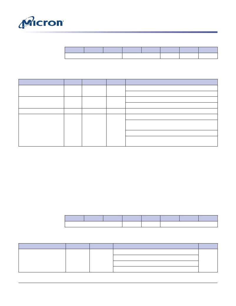
�Table� 11:� MR0� Device� Information� (MA[7:0]� =� 00h)�
�OP7�
�OP6�
�OP5�
�OP4�
�OP3�
�OP2�
�OP1�
�OP0�
�RFU�
�RZQI�
�DNVI�
�DI�
�DAI�
�Table� 12:� MR0� Op-Code� Bit� Definitions�
�Notes� 1–4� apply� to� all� parameters� and� conditions�
�Register� Information�
�Device� auto� initialization�
�Tag�
�DAI�
�Type�
�Read-only�
�OP�
�OP0�
�Definition�
�0b:� DAI� complete�
�status�
�1b:� DAI� in� progress�
�Device� information�
�DI�
�Read-only�
�OP1�
�0b�
�1b:� NVM�
�Data not valid information�
�Built-in� self� test� for� RZQ�
�DNVI�
�RZQI�
�Read-only�
�Read-only�
�OP2�
�OP[4:3]�
�0b:� DNVI� not� supported�
�00b:� RZQ� self� test� not� supported�
�information�
�Notes:�
�01b:� ZQ� pin� might� be� connected� to� V� DDCA� or� left� float-�
�ing�
�10b:� ZQ� pin� might� be� shorted� to� ground�
�11b:� ZQ� pin� self� test� complete;� no� error� condition� de-�
�tected�
�1.� If� RZQI� is� supported,� it� will� be� set� upon� completion� of� the� MRW� ZQ� initialization� calibra-�
�tion.�
�2.� If� ZQ� is� connected� to� V� DDCA� to� set� default� calibration,� OP[4:3]� must� be� set� to� 01.� If� ZQ� is�
�not� connected� to� V� DDCA� ,� either� OP[4:3]� =� 01� or� OP[4:3]� =� 10� could� indicate� a� ZQ-pin� as-�
�sembly� error.� It� is� recommended� that� the� assembly� error� be� corrected.�
�3.� In� the� case� of� a� possible� assembly� error� (either� OP[4:3]� =� 01� or� OP[4:3]� =� 10,� as� defined�
�above),� the� device� will� default� to� factory� trim� settings� for� R� ON� and� will� ignore� ZQ� cali-�
�bration� commands.� In� either� case,� the� system� might� not� function� as� intended.�
�4.� If� a� ZQ� self� test� returns� a� value� of� 11b,� this� indicates� that� the� device� has� detected� a� resis-�
�tor� connection� to� the� ZQ� pin.� Note� that� this� result� cannot� be� used� to� validate� the� ZQ�
�resistor� value,� nor� does� it� indicate� that� the� ZQ� resistor� tolerance� meets� the� specified� lim-�
�its� (240� ohms� ±1%).�
�Table� 13:� MR1� Device� Feature� 1� (MA[7:0]� =� 01h)�
�OP7�
�OP6�
�OP5�
�OP4�
�OP3�
�OP2�
�OP1�
�OP0�
�n� WR� (for� AP)�
�WC�
�BT�
�BL�
�Table� 14:� MR1� Op-Code� Bit� Definitions�
�Feature�
�BL� =� burst� length�
�Type�
�Write-only�
�OP�
�OP[2:0]�
�Definition�
�010b:� BL4� (default)�
�Notes�
�011b:� BL8�
�100b:� BL16�
�All� others:� Reserved�
�PDF:� 09005aef83f3f2eb�
�2gb_mobile_lpddr2_s4_g69a.pdf� –� Rev.� N� 3/12� EN�
�45�
�Micron� Technology,� Inc.� reserves� the� right� to� change� products� or� specifications� without� notice.�
�2010� Micron� Technology,� Inc.� All� rights� reserved.�
�相关PDF资料 |
PDF描述 |
|---|---|
| P51-300-G-H-I12-20MA-000-000 | SENSOR 300PSI M12-1.5 6G 4-20MA |
| REC5-0509SRW/H2/A/M/SMD | CONV DC/DC 5W 4.5-9VIN 09VOUT |
| P51-500-A-H-P-4.5OVP-000-000 | SENSOR 500PSI M12-1.5 6G .5-4.5V |
| P51-300-A-AD-D-20MA-000-000 | SENSOR 300PSI 7/16-20 UNF 4-20MA |
| P51-300-A-H-P-4.5OVP-000-000 | SENSOR 300PSI M12-1.5 6G .5-4.5V |
相关代理商/技术参数 |
参数描述 |
|---|
发布紧急采购,3分钟左右您将得到回复。