- 您现在的位置:买卖IC网 > PDF目录21087 > MT42L256M32D4MG-25 IT:A (Micron Technology Inc)IC LPDDR2 SDRAM 8GBIT 134FBGA PDF资料下载
参数资料
| 型号: | MT42L256M32D4MG-25 IT:A |
| 厂商: | Micron Technology Inc |
| 文件页数: | 62/164页 |
| 文件大小: | 0K |
| 描述: | IC LPDDR2 SDRAM 8GBIT 134FBGA |
| 标准包装: | 1,000 |
| 格式 - 存储器: | RAM |
| 存储器类型: | 移动 LPDDR2 SDRAM |
| 存储容量: | 8G(356M x 32) |
| 速度: | 400MHz |
| 接口: | 并联 |
| 电源电压: | 1.14 V ~ 1.3 V |
| 工作温度: | -25°C ~ 85°C |
| 封装/外壳: | 134-TFBGA |
| 供应商设备封装: | 134-FBGA(11.5x11.5) |
| 包装: | 散装 |
第1页第2页第3页第4页第5页第6页第7页第8页第9页第10页第11页第12页第13页第14页第15页第16页第17页第18页第19页第20页第21页第22页第23页第24页第25页第26页第27页第28页第29页第30页第31页第32页第33页第34页第35页第36页第37页第38页第39页第40页第41页第42页第43页第44页第45页第46页第47页第48页第49页第50页第51页第52页第53页第54页第55页第56页第57页第58页第59页第60页第61页当前第62页第63页第64页第65页第66页第67页第68页第69页第70页第71页第72页第73页第74页第75页第76页第77页第78页第79页第80页第81页第82页第83页第84页第85页第86页第87页第88页第89页第90页第91页第92页第93页第94页第95页第96页第97页第98页第99页第100页第101页第102页第103页第104页第105页第106页第107页第108页第109页第110页第111页第112页第113页第114页第115页第116页第117页第118页第119页第120页第121页第122页第123页第124页第125页第126页第127页第128页第129页第130页第131页第132页第133页第134页第135页第136页第137页第138页第139页第140页第141页第142页第143页第144页第145页第146页第147页第148页第149页第150页第151页第152页第153页第154页第155页第156页第157页第158页第159页第160页第161页第162页第163页第164页
�� �
�
�2Gb:� x16,� x32� Mobile� LPDDR2� SDRAM� S4�
�Burst� WRITE� Command�
�every� eighth� clock� cycle� for� BL� =� 16� operation.� This� operation� is� supported� as� long� as� the�
�banks� are� activated,� whether� the� accesses� read� the� same� or� different� banks.�
�READs� Interrupted� by� a� READ�
�A� burst� READ� can� be� interrupted� by� another� READ� with� a� 4-bit� burst� boundary,� provi-�
�ded� that� t� CCD� is� met.�
�A� burst� READ� can� be� interrupted� by� other� READs� on� any� subsequent� clock,� provided�
�that� t� CCD� is� met.�
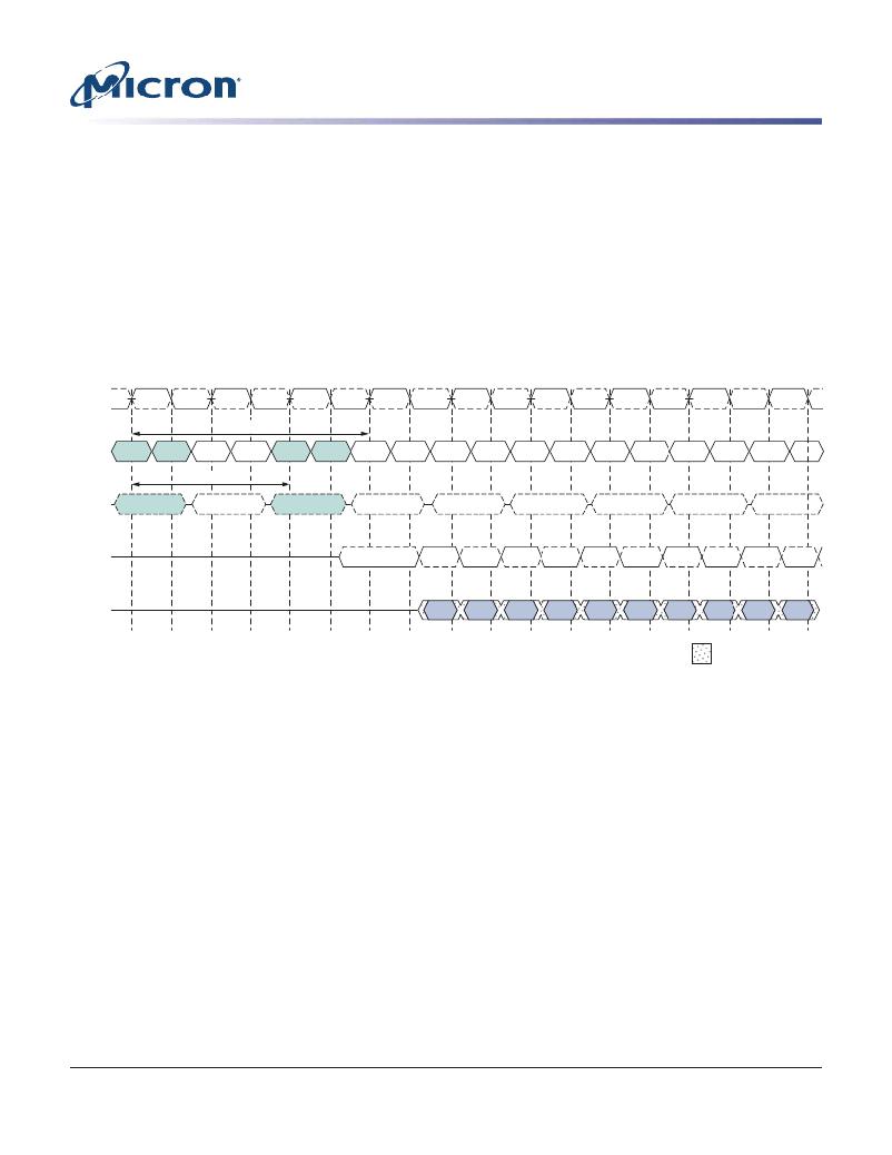
�Figure� 38:� READ� Burst� Interrupt� Example� –� RL� =� 3,� BL� =� 8,� t� CCD� =� 2�
�T0�
�T1�
�T2�
�T3�
�T4�
�T5�
�T6�
�T7�
�T8�
�CK#�
�CK�
�RL� =� 3�
�CA[9:0]�
�Bank� n�
�col� addr� a�
�Col� addr� a�
�Bank� n�
�col� addr� b�
�Col� addr� b�
�t� CCD�
�=2�
�CMD�
�READ�
�NOP�
�READ�
�NOP�
�NOP�
�NOP�
�NOP�
�NOP�
�NOP�
�DQS#�
�DQS�
�DQ�
�D� OUT� A0�
�D� OUT� A1�
�D� OUT� A2�
�D� OUT� A3�
�D� OUT� B0�
�D� OUT� B1�
�D� OUT� B2�
�D� OUT� B3�
�D� OUT� B4�
�D� OUT� B5�
�Transitioning� data�
�Note:�
�1.� READs� can� only� be� interrupted� by� other� READs� or� the� BST� command.�
�Burst� WRITE� Command�
�The� burst� WRITE� command� is� initiated� with� CS#� LOW,� CA0� HIGH,� CA1� LOW,� and� CA2�
�LOW� at� the� rising� edge� of� the� clock.� The� command� address� bus� inputs,� CA5r–CA6r� and�
�CA1f–CA9f,� determine� the� starting� column� address� for� the� burst.� Write� latency� (WL)� is�
�defined� from� the� rising� edge� of� the� clock� on� which� the� WRITE� command� is� issued� to� the�
�rising� edge� of� the� clock� from� which� the� t� DQSS� delay� is� measured.� The� first� valid� data�
�must� be� driven� WL� � t� CK� +� t� DQSS� from� the� rising� edge� of� the� clock� from� which� the�
�WRITE� command� is� issued.� The� data� strobe� signal� (DQS)� must� be� driven� LOW� t� WPRE�
�prior� to� data� input.� The� burst� cycle� data� bits� must� be� applied� to� the� DQ� pins� t� DS� prior� to�
�the� associated� edge� of� the� DQS� and� held� valid� until� t� DH� after� that� edge.� Burst� data� is�
�sampled� on� successive� edges� of� the� DQS� until� the� 4-,� 8-,� or� 16-bit� burst� length� is� com-�
�pleted.� After� a� burst� WRITE� operation,� t� WR� must� be� satisfied� before� a� PRECHARGE�
�command� to� the� same� bank� can� be� issued.�
�Pin� input� timings� are� measured� relative� to� the� crosspoint� of� DQS� and� its� complement,�
�DQS#.�
�PDF:� 09005aef83f3f2eb�
�2gb_mobile_lpddr2_s4_g69a.pdf� –� Rev.� N� 3/12� EN�
�62�
�Micron� Technology,� Inc.� reserves� the� right� to� change� products� or� specifications� without� notice.�
�2010� Micron� Technology,� Inc.� All� rights� reserved.�
�相关PDF资料 |
PDF描述 |
|---|---|
| P51-300-G-H-I12-20MA-000-000 | SENSOR 300PSI M12-1.5 6G 4-20MA |
| REC5-0509SRW/H2/A/M/SMD | CONV DC/DC 5W 4.5-9VIN 09VOUT |
| P51-500-A-H-P-4.5OVP-000-000 | SENSOR 500PSI M12-1.5 6G .5-4.5V |
| P51-300-A-AD-D-20MA-000-000 | SENSOR 300PSI 7/16-20 UNF 4-20MA |
| P51-300-A-H-P-4.5OVP-000-000 | SENSOR 300PSI M12-1.5 6G .5-4.5V |
相关代理商/技术参数 |
参数描述 |
|---|
发布紧急采购,3分钟左右您将得到回复。