- 您现在的位置:买卖IC网 > PDF目录385639 > MT46V64M8 (Micron Technology, Inc.) 16 Meg x 8 x 4 banks DDR SDRAM(16M x 8 x 4组,双数据速率同步动态RAM) PDF资料下载
参数资料
| 型号: | MT46V64M8 |
| 厂商: | Micron Technology, Inc. |
| 英文描述: | 16 Meg x 8 x 4 banks DDR SDRAM(16M x 8 x 4组,双数据速率同步动态RAM) |
| 中文描述: | 16梅格× 8 × 4银行DDR SDRAM内存(1,600 × 8 × 4组,双数据速率同步动态RAM)的 |
| 文件页数: | 48/70页 |
| 文件大小: | 2524K |
| 代理商: | MT46V64M8 |
第1页第2页第3页第4页第5页第6页第7页第8页第9页第10页第11页第12页第13页第14页第15页第16页第17页第18页第19页第20页第21页第22页第23页第24页第25页第26页第27页第28页第29页第30页第31页第32页第33页第34页第35页第36页第37页第38页第39页第40页第41页第42页第43页第44页第45页第46页第47页当前第48页第49页第50页第51页第52页第53页第54页第55页第56页第57页第58页第59页第60页第61页第62页第63页第64页第65页第66页第67页第68页第69页第70页
48
512Mb: x4, x8, x16 DDR SDRAM
512Mx4x8x16DDR_A.p65
–
Rev. A; Pub 10/00
Micron Technology, Inc., reserves the right to change products or specifications without notice.
2000, Micron Technology, Inc.
512Mb: x4, x8, x16
DDR SDRAM
ADVANCE
(continued on following page)
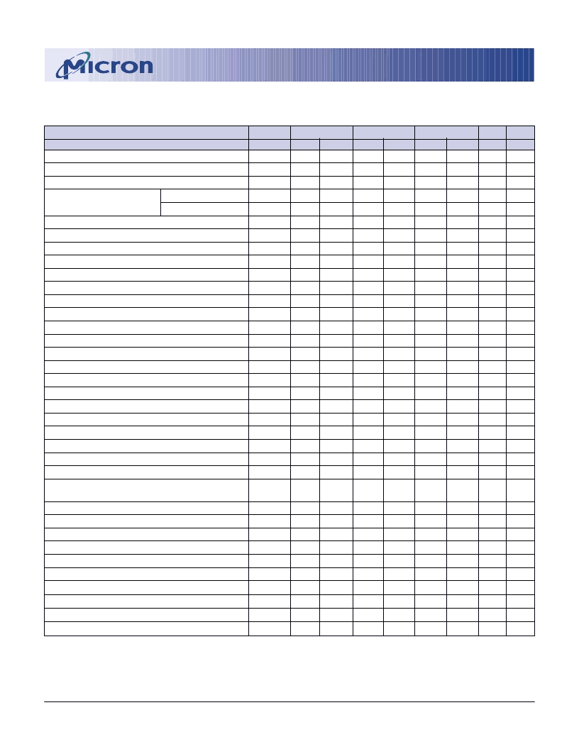
ELECTRICAL CHARACTERISTICS AND RECOMMENDED AC OPERATING CONDITIONS
(Notes: 1
–
5, 14-17, 33; notes appear on pages 50
–
53) (0
°
C
≤
T
A
≤
+70
°
C; V
DD
Q = +2.5V ±0.2V, V
DD
= +2.5V ±0.2V)
AC CHARACTERISTICS
PARAMETER
Access window of DQs from CK/CK#
CK high-level width
CK low-level width
Clock cycle time
-7
-75
-8
SYMBOL
t
AC
t
CH
t
CL
t
CK(2.5)
t
CK(2)
t
DH
t
DS
t
DIPW
t
DQSCK
t
DQSH
t
DQSL
t
DQSQ
t
DQSQA
t
DQSS
t
DSS
t
DSH
t
HP
t
HZ
t
LZ
t
IH
F
t
IS
F
t
IH
S
t
IH
S
t
IPW
t
MRD
t
QH
MIN
-0.75
0.45
0.45
7
7.5
0.5
0.5
1.75
-0.75
0.35
0.35
MAX
+0.75
0.55
0.55
12
12
MIN
-0.75
0.45
0.45
7.5
10
0.5
0.5
1.75
-0.75
0.35
0.35
MAX
+0.75
0.55
0.55
12
12
MIN
-0.8
0.45
0.45
8
10
0.6
0.6
2
-0.8
0.35
0.35
MAX
+0.8
0.55
0.55
12
12
UNITS NOTES
ns
t
CK
t
CK
ns
ns
ns
ns
ns
ns
t
CK
t
CK
ns
ns
t
CK
t
CK
t
CK
ns
ns
ns
ns
ns
ns
ns
ns
ns
ns
30
30
52
52
CL = 2.5
CL = 2
DQ and DM input hold time relative to DQS
DQ and DM input setup time relative to DQS
DQ and DM input pulse width (for each input)
Access window of DQS from CK/CK#
DQS input high pulse width
DQS input low pulse width
DQS-DQ skew, DQS to last DQ valid, per group, per access
DQS-DQ skew, first DQS to last DQ valid, per access
Write command to first DQS latching transition
DQS falling edge to CK rising - setup time
DQS falling edge from CK rising - hold time
Half clock period
Data-out high-impedance window from CK/CK#
Data-out low-impedance window from CK/CK#
Address and control input hold time (fast slew rate)
Address and control input setup time (fast slew rate)
Address and control input hold time (slow slew rate)
Address and control input setup time (slow slew rate)
Address and control input pulse width
LOAD MODE REGISTER command cycle time
DQ-DQS hold, DQS to first DQ to go non-valid, per access
26, 31
26, 31
31
+0.75
+0.75
+0.8
0.5
0.7
1.25
0.5
0.7
1.25
0.6
0.8
1.25
25, 26
36
0.75
0.2
0.2
t
CH,
t
CL
-0.75
-0.75
.90
.90
1
1
2.2
15
t
HP
-
t
QHS
0.75
0.2
0.2
t
CH,
t
CL
-0.75
-0.75
.90
.90
1
1
2.2
15
t
HP
-
t
QHS
0.75
0.2
0.2
t
CH,
t
CL
-0.8
-0.8
1.1
1.1
1.1
1.1
2.5
16
t
HP
-
t
QHS
34
18
18
14
14
14
14
+0.75
+0.75
+0.75
+0.75
+0.8
+0.8
25, 26,
34
Data hold skew factor
ACTIVE to PRECHARGE command
ACTIVE to READ with Auto precharge command
ACTIVE to ACTIVE/AUTO REFRESH command period
AUTO REFRESH command period
ACTIVE to READ or WRITE delay
t
QHS
t
RAS
t
RAP
t
RC
t
RFC
t
RCD
0.75
120,000
0.75
120,000
1
ns
ns
ns
ns
ns
ns
45
15
60
67
15
45
20
65
75
20
50
20
70
80
20
120,000
35
50
PRECHARGE command period
t
RP
t
RPRE
t
RPST
t
RRD
15
20
20
ns
t
CK
t
CK
t
CK
DQS read preamble
DQS read postamble
ACTIVE bank
a
to ACTIVE bank
b
command
0.9
0.4
2
1.1
0.6
0.9
0.4
2
1.1
0.6
0.9
0.4
2
1.1
0.6
42
相关PDF资料 |
PDF描述 |
|---|---|
| MT48LC16M8A1TG | SYNCHRONOUS DRAM |
| MT48LC32M4A1 | ECONOLINE: RSZ/P - 1kVDC |
| MT48LC32M4A2 | SYNCHRONOUS DRAM |
| MT48LC32M4A1TG | SYNCHRONOUS DRAM |
| MT48LC8M16A1TG | SYNCHRONOUS DRAM |
相关代理商/技术参数 |
参数描述 |
|---|
发布紧急采购,3分钟左右您将得到回复。