- 您现在的位置:买卖IC网 > PDF目录385639 > MT46V64M8 (Micron Technology, Inc.) 16 Meg x 8 x 4 banks DDR SDRAM(16M x 8 x 4组,双数据速率同步动态RAM) PDF资料下载
参数资料
| 型号: | MT46V64M8 |
| 厂商: | Micron Technology, Inc. |
| 英文描述: | 16 Meg x 8 x 4 banks DDR SDRAM(16M x 8 x 4组,双数据速率同步动态RAM) |
| 中文描述: | 16梅格× 8 × 4银行DDR SDRAM内存(1,600 × 8 × 4组,双数据速率同步动态RAM)的 |
| 文件页数: | 53/70页 |
| 文件大小: | 2524K |
| 代理商: | MT46V64M8 |
第1页第2页第3页第4页第5页第6页第7页第8页第9页第10页第11页第12页第13页第14页第15页第16页第17页第18页第19页第20页第21页第22页第23页第24页第25页第26页第27页第28页第29页第30页第31页第32页第33页第34页第35页第36页第37页第38页第39页第40页第41页第42页第43页第44页第45页第46页第47页第48页第49页第50页第51页第52页当前第53页第54页第55页第56页第57页第58页第59页第60页第61页第62页第63页第64页第65页第66页第67页第68页第69页第70页
53
512Mb: x4, x8, x16 DDR SDRAM
512Mx4x8x16DDR_A.p65
–
Rev. A; Pub 10/00
Micron Technology, Inc., reserves the right to change products or specifications without notice.
2000, Micron Technology, Inc.
512Mb: x4, x8, x16
DDR SDRAM
ADVANCE
NOTES (continued)
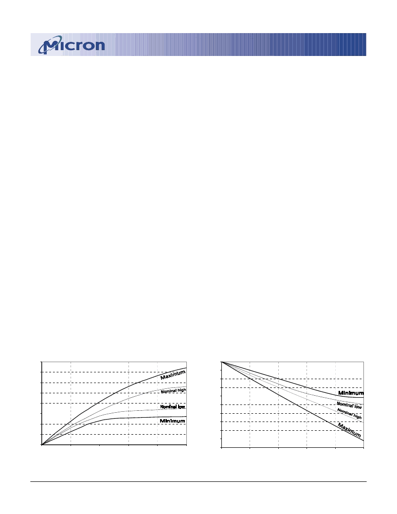
38.Reduced Output Drive Curves:
a) The full variation in driver pull-down current from
minimum to maximum process, temperature and
voltage will lie within the outer bounding lines of
the V-I curve of Figure C.
b) The variation in driver pull-down current
within nominal limits of voltage and tempera-
ture is expected, but not guaranteed, to lie
within the inner bounding lines of the V-I
curve of Figure C.
c) The full variation in driver pull-up current from
minimum to maximum process, temperature and
voltage will lie within the outer bounding lines of
the V-I curve of Figure D.
d) The variation in driver pull-up current within
nominal limits of voltage and temperature is
expected, but not guaranteed, to lie within
the inner bounding lines of the V-I curve of
Figure D.
e) The full variation in the ratio of the maximum
to minimum pull-up and pull-down current
should be between .71 and 1.4 for device
drain-to-source voltages from 0.1V to 1.0
Volt, and at the same voltage and tempera-
ture.
f) The full variation in the ratio of the nominal
pull-up to pull-down current should be unity
±10%, for device drain-to-source voltages
from 0.1V to 1.0 Volt.
39. The voltage levels used are derived from the
refernced test load. In practice, the voltage levels
obtained from a properly terminated bus will
provide significantly different voltage values.
40. V
IH
overshoot: V
IH
(MAX) = V
DD
Q+1.5V for a
pulse width
≤
3ns and the pulse width can not
be greater than 1/3 of the cycle rate.
Figure C
Pull-Dow n Characteristics
0
10
20
30
40
50
60
70
80
0.0
0.5
1.0
1.5
2.0
2.5
V
OUT
(V)
I
O
Figure D
Pull-Up Characteristics
-50
-45
-40
-35
-30
-25
-20
-15
-10
-5
0
0.0
0.2
0.4
0.6
0.8
1.0
V
DD
Q - V
OUT
(V)
I
O
VIL undershoot: VIL(MIN) = -1.5V for a pulse
width
≤
3ns and the pulse width can not be
greater than 1/3 of the cycle rate.
41. V
DD
and V
DDQ
must track each other.
42. Note 42 is not used.
43. Note 43 is not used.
44. During initialization, V
DDQ
,
V
TT
,
and V
REF
must be
equal to or less than V
DD
+ 0.3V.
Alternatively,
V
TT
may be 1.35V maximum during power up,
even if V
DD
/ V
DDQ
are 0 volts,
provided a
minimum of 42 ohms of series resistance is used
between the V
TT
supply and the input pin.
45. Note 45 is not used.
46. Note 46 is not used.
47.
Note 47 is not used.
48. Random addressing changing 50% of data
changing at every transfer.
49. Random addressing changing 100% of data
changing at every transfer.
50. CKE must be active (high) during the entire time
a refresh command is executed. That is, from the
time the AUTO REFRESH command is registered,
CKE must be active at each rising clock edge,
until
t
REF later.
51. IDD2N specifies the DQ, DQS, and DM to be
driven to a valid high or low logic level. IDD2Q
is similar to IDD2F except IDD2Q specifies the
address and control inputs to remain stable.
Although IDD2F, IDD2N, and IDD2Q are
similar, IDD2F is “worst case.”
52. Whenever the operating frequency is altered, not
including jitter, the DLL is required to be reset,
and followed by 200 clock cycles.
相关PDF资料 |
PDF描述 |
|---|---|
| MT48LC16M8A1TG | SYNCHRONOUS DRAM |
| MT48LC32M4A1 | ECONOLINE: RSZ/P - 1kVDC |
| MT48LC32M4A2 | SYNCHRONOUS DRAM |
| MT48LC32M4A1TG | SYNCHRONOUS DRAM |
| MT48LC8M16A1TG | SYNCHRONOUS DRAM |
相关代理商/技术参数 |
参数描述 |
|---|
发布紧急采购,3分钟左右您将得到回复。