- 您现在的位置:买卖IC网 > PDF目录385639 > MT46V64M8 (Micron Technology, Inc.) 16 Meg x 8 x 4 banks DDR SDRAM(16M x 8 x 4组,双数据速率同步动态RAM) PDF资料下载
参数资料
| 型号: | MT46V64M8 |
| 厂商: | Micron Technology, Inc. |
| 英文描述: | 16 Meg x 8 x 4 banks DDR SDRAM(16M x 8 x 4组,双数据速率同步动态RAM) |
| 中文描述: | 16梅格× 8 × 4银行DDR SDRAM内存(1,600 × 8 × 4组,双数据速率同步动态RAM)的 |
| 文件页数: | 60/70页 |
| 文件大小: | 2524K |
| 代理商: | MT46V64M8 |
第1页第2页第3页第4页第5页第6页第7页第8页第9页第10页第11页第12页第13页第14页第15页第16页第17页第18页第19页第20页第21页第22页第23页第24页第25页第26页第27页第28页第29页第30页第31页第32页第33页第34页第35页第36页第37页第38页第39页第40页第41页第42页第43页第44页第45页第46页第47页第48页第49页第50页第51页第52页第53页第54页第55页第56页第57页第58页第59页当前第60页第61页第62页第63页第64页第65页第66页第67页第68页第69页第70页
60
512Mb: x4, x8, x16 DDR SDRAM
512Mx4x8x16DDR_A.p65
–
Rev. A; Pub 10/00
Micron Technology, Inc., reserves the right to change products or specifications without notice.
2000, Micron Technology, Inc.
512Mb: x4, x8, x16
DDR SDRAM
ADVANCE
TIMING PARAMETERS
-7
-75
-8
SYMBOL
t
CH
t
CL
t
CK (2.5)
t
CK (2)
t
IH
MIN
0.45
0.45
7
7.5
1
MAX
0.55
0.55
12
12
MIN
0.45
0.45
7.5
10
1
MAX
0.55
0.55
12
2
MIN
0.45
0.45
8
10
1.1
MAX
0.55
0.55
12
12
UNITS
t
CK
t
CK
ns
ns
ns
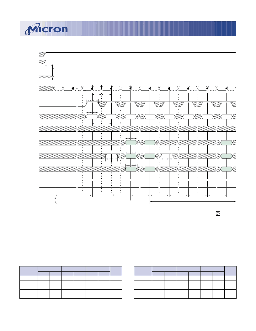
INITIALIZE AND LOAD MODE REGISTERS
-7
-75
-8
SYMBOL
t
IS
t
MRD
t
RFC
t
RP
t
VTD
MIN
1
15
67
15
0
MAX
MIN
1
15
75
20
0
MAX
MIN
1.1
16
80
20
0
MAX
UNITS
ns
ns
ns
ns
ns
t
VTD
1
CKE
LVCMOS
LOW LEVEL
DQ
BA0, BA1
200 cycles of CK
3
Load Extended
Mode Register
Load Mode
Register
2
tMRD
tMRD
tRP
tRFC
tRFC
5
t
IS
Power-up:
V
DD
and
CK stable
T = 200μs
High-Z
t
IH
(
)
(
)
(
)
(
)
(
)
(
)
(
)
(
)
(
)
(
)
(
)
(
)
(
)
(
)
(
)
(
)
(
)
(
)
(
)
(
)
(
)
(
)
(
)
(
)
(
)
(
)
(
)
(
)
(
)
(
)
(
)
(
)
(
)
(
)
(
)
(
)
(
)
(
)
(
)
(
)
(
)
(
)
(
)
(
)
(
)
(
)
(
)
(
)
(
)
(
)
(
)
(
)
(
)
(
)
(
)
(
)
(
)
(
)
(
)
(
)
(
)
(
)
(
)
(
)
(
)
(
)
(
)
(
)
(
)
(
)
(
)
(
)
DM
(
)
(
)
(
)
(
)
(
)
(
)
(
)
(
)
DQS
High-Z
A0-A9, A11, A12
RA
A10
RA
ALL BANKS
CK
CK#
t
CH
t
CL
t
CK
V
TT
1
V
REF
V
DD
V
DD
Q
COMMAND
6
LMR
NOP
PRE
LMR
AR
(
)
(
)
(
)
(
)
AR
ACT
5
tIS
tIH
BA1 = L
tIS
tIH
t
IS
t
IH
BA1 = L
tIS
tIH
(
)
(
)
(
)
(
)
(
)
(
)
(
)
(
)
(
)
(
)
(
)
(
)
(
)
(
)
(
)
(
)
(
)
(
)
(
)
(
)
CODE
CODE
tIS
tIH
CODE
CODE
(
)
(
)
(
)
(
)
PRE
ALL BANKS
tIS
tIH
NOTE:
1. V
TT
is not applied directly to the device; however, tVTD should be greater than or equal to zero to avoid device latch-up. V
DD
Q
,
V
DD
Q, V
TT
and V
REF
must be equal to or less than V
DD
+ 0.3V. Alternatively, V
TT
may be 1.35V maximum during power up, even if
V
DD
/V
DD
Q are 0 volts, provided a minimum of 42 ohms of series resistance is used between the V
TT
supply and the input pin.
2. Although not required by the Micron device, JEDEC specifies resetting the DLL with A8 = H.
3. tMRD is required before any command can be applied, and 200 cycles of CK are required before a READ command can be issued.
4. The two AUTO REFRESH commands at Tc0 and Td0 may be applied after the LOAD MODE REGISTER (LMR) command at Ta0.
5. Although not required by the Micron device, JEDEC specifies issuing another LMR command (A8 = L) prior to activating any bank.
6. PRE = PRECHARGE command, LMR = LOAD MODE REGISTER command, AR = AUTO REFRESH command, ACT = ACTIVE command,
RA = Row Address, Bank Address
(
)
(
)
(
)
(
)
T0
T1
T2
Ta0
Tb0
Tc0
Td0
Te0
(
)
(
)
(
)
(
)
(
)
(
)
DON
’
T CARE
BA
(
)
(
)
(
)
(
)
(
)
(
)
(
)
(
)
(
)
(
)
(
)
(
)
(
)
(
)
(
)
(
)
(
)
(
)
(
)
(
)
(
)
(
)
(
)
(
)
(
)
(
)
(
)
(
)
(
)
(
)
(
)
(
)
(
)
(
)
(
)
(
)
(
)
(
)
(
)
(
)
(
)
(
)
(
)
(
)
(
)
(
)
(
)
(
)
()()
(
)
(
)
(
)
(
)
()()
()()
()()
()()
()()
()()
()()
()()
()()
(
)
(
)
(
)
(
)
(
)
(
)
(
)
(
)
(
)
(
)
(
)
(
)
(
)
(
)
(
)
(
)
(
)
(
)
(
)
(
)
(
)
(
)
(
)
(
)
(
)
(
)
(
)
(
)
()()
()()
tRP
相关PDF资料 |
PDF描述 |
|---|---|
| MT48LC16M8A1TG | SYNCHRONOUS DRAM |
| MT48LC32M4A1 | ECONOLINE: RSZ/P - 1kVDC |
| MT48LC32M4A2 | SYNCHRONOUS DRAM |
| MT48LC32M4A1TG | SYNCHRONOUS DRAM |
| MT48LC8M16A1TG | SYNCHRONOUS DRAM |
相关代理商/技术参数 |
参数描述 |
|---|
发布紧急采购,3分钟左右您将得到回复。