- 您现在的位置:买卖IC网 > PDF目录132985 > MTA85812S-10I/SS 8-BIT, OTPROM, 10 MHz, RISC MICROCONTROLLER, PDSO20 PDF资料下载
参数资料
| 型号: | MTA85812S-10I/SS |
| 元件分类: | 微控制器/微处理器 |
| 英文描述: | 8-BIT, OTPROM, 10 MHz, RISC MICROCONTROLLER, PDSO20 |
| 封装: | 0.209 INCH, PLASTIC, SSOP-20 |
| 文件页数: | 31/72页 |
| 文件大小: | 760K |
| 代理商: | MTA85812S-10I/SS |
第1页第2页第3页第4页第5页第6页第7页第8页第9页第10页第11页第12页第13页第14页第15页第16页第17页第18页第19页第20页第21页第22页第23页第24页第25页第26页第27页第28页第29页第30页当前第31页第32页第33页第34页第35页第36页第37页第38页第39页第40页第41页第42页第43页第44页第45页第46页第47页第48页第49页第50页第51页第52页第53页第54页第55页第56页第57页第58页第59页第60页第61页第62页第63页第64页第65页第66页第67页第68页第69页第70页第71页第72页
1995 Microchip Technology Inc.
DS40115C-page 37
MTA85XXX
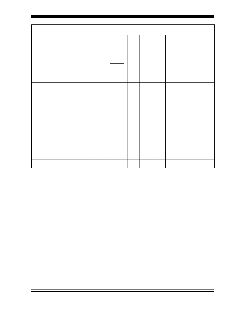
T0CKI Input Timing,
With prescaler
T0CKI High Pulse Width
TRTH
10*
ns
Note 3
T0CKI Low Pulse Width
TRTL
10*
ns
Note 3
T0CKI period
TRTP
TCY +40*
N
ns
Note 3. Where N = prescale
value (2,4,...,256)
Watchdog Timer Time-out Period,
No prescaler
TWDT
9*
18*
30*
ms
VDD = 5.0V
Oscillation Start-up Timer Period TOST
9*
18*
30*
ms
VDD = 5.0V
I/O Timing
I/O pin input valid before
CLKOUT
↑ (RC mode)
TDS
0.25 TCY+30*
ns
I/O Pin input hold after CLKOUT
↑
(RC mode)
TDH
0*
ns
I/O pin output valid after CLKOUT
↓
(RC Mode)
TPD
40*
ns
I/O pin input valid before OSC
↑
(I/O setup time)
TioV2osH
TBD
ns
OSC1
↑ to I/O pin input invalid
(I/O holdup time)
TosH2ioL
TBD
ns
OSC1
↑ to I/O pin output valid
TosH2ioV
TBD
ns
I/O pin output rise time
TioR
TBD
ns
I/O pin output fall time
TioF
TBD
ns
Capacitive loading specs on
output pins
OSC2 pin
COSC215
pF
In Xt, HS or LP modes when
external clock is used to drive
OSC1
All I/O pins
CIO
50
pF
Excludes RB7 on MTA85X1X
devices
AC CHARACTERISTICS
Standard Operating Conditions
Operating temperature
-40
°C ≤ TA ≤ +85°C for industrial
Characteristic
Sym
Min
Typ
Max
Units
Conditions
* Guaranteed by characterization but not tested.
Note 1: Data in the column labeled "Typ" is based on characterization results at 25
°C. This data is for design guidance
only and is not tested for, or guaranteed by Microchip Technology.
Note 2: Instruction cycle period (TCY) equals four times the input oscillator time base period. All specified values are
based on characterization data for that particular oscillator type under standard operating conditions with the
device executing code. Exceeding these specified limits may result in unstable oscillator operation and/or
higher than expected current consumption. All devices are tested to operate at "minimum" values with an
external clock applied to the OSC1 pin. When an external clock input is used, the "maximum" cycle time limit
is "DC" (no clock) for all devices.
Note 3: For a detailed explanation of T0CKI input clock requirements see microcontroller datasheet Section 5.2.1.
Note 4: Clock-in high-time is the duration for which clock input is at VIHOSC or higher.
Clock-in low-time is the duration for which clock input is at VILOSC or lower.
Note 5: This HS specification is only for the -20 device. The -10 device has a maximum of 10 MHz and the -04 device
has a maximum of 4 MHz.
相关PDF资料 |
PDF描述 |
|---|---|
| MB91661PMC | 32-BIT, MROM, 33 MHz, RISC MICROCONTROLLER, PQFP120 |
| MPC8266ACZULHDX | 32-BIT, 250 MHz, RISC PROCESSOR, PBGA480 |
| MPC8266ACZUPIBX | 32-BIT, 300 MHz, RISC PROCESSOR, PBGA480 |
| MPC8266AZULHDX | 32-BIT, 250 MHz, RISC PROCESSOR, PBGA480 |
| MPC8266AZUPIBX | 32-BIT, 300 MHz, RISC PROCESSOR, PBGA480 |
相关代理商/技术参数 |
参数描述 |
|---|---|
| MTA8808 | 制造商:Pulse Electronics Corporation 功能描述: |
| MTA8ATF1G64AZ-2G3B1 | 功能描述:Memory Module DDR4 SDRAM 8GB 2400MT/s 288-UDIMM 制造商:micron technology inc. 系列:- 零件状态:在售 存储器类型:DDR4 SDRAM 存储容量:8GB 速度:2400MT/s 封装/外壳:288-UDIMM 标准包装:1 |
| MTA8ATF1G64HZ-2G3B1 | 功能描述:Memory Module DDR4 SDRAM 8GB 2400MT/s 260-SODIMM 制造商:micron technology inc. 系列:- 零件状态:在售 存储器类型:DDR4 SDRAM 存储容量:8GB 速度:2400MT/s 封装/外壳:260-SODIMM 标准包装:1 |
| MTA8D50 | 制造商:Mallory Sonalert Products Inc 功能描述:Molded Tubular Aluminum Electrolytic Axial Leads Capacitor - 8uF 50dcV -10+100% |
| MTA90A | 制造商:LIUJING 制造商全称:LIUJING 功能描述:可控硅(晶闸管) |
发布紧急采购,3分钟左右您将得到回复。