- 您现在的位置:买卖IC网 > PDF目录189448 > OR3L165B8PS208-DB (LATTICE SEMICONDUCTOR CORP) FPGA, 1024 CLBS, 120000 GATES, 333 MHz, PQFP208 PDF资料下载
参数资料
| 型号: | OR3L165B8PS208-DB |
| 厂商: | LATTICE SEMICONDUCTOR CORP |
| 元件分类: | FPGA |
| 英文描述: | FPGA, 1024 CLBS, 120000 GATES, 333 MHz, PQFP208 |
| 封装: | SQFP2-208 |
| 文件页数: | 38/77页 |
| 文件大小: | 873K |
| 代理商: | OR3L165B8PS208-DB |
第1页第2页第3页第4页第5页第6页第7页第8页第9页第10页第11页第12页第13页第14页第15页第16页第17页第18页第19页第20页第21页第22页第23页第24页第25页第26页第27页第28页第29页第30页第31页第32页第33页第34页第35页第36页第37页当前第38页第39页第40页第41页第42页第43页第44页第45页第46页第47页第48页第49页第50页第51页第52页第53页第54页第55页第56页第57页第58页第59页第60页第61页第62页第63页第64页第65页第66页第67页第68页第69页第70页第71页第72页第73页第74页第75页第76页第77页
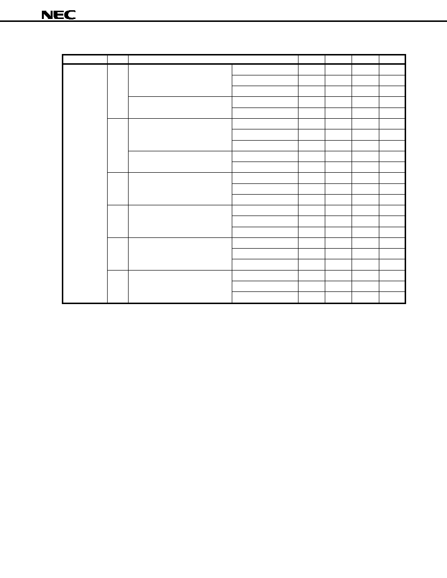
43
PD78052, 78053, 78054, 78055, 78056, 78058
Data Sheet U12327EJ5V0DS00
DC Characteristics (TA = –40 to +85
°C, VDD = 2.0 to 6.0 V)
Parameter
Symbol
Conditions
MIN.
TYP.
MAX.
Unit
Power supply
IDD1
5.0 MHz crystal oscillation operating
VDD = 5.0 V
±10%Note 5
412
mA
currentNote 1
mode (fXX = 2.5 MHz)Note 2
VDD = 3.0 V
±10%Note 6
0.6
1.8
mA
VDD = 2.2 V
±10%Note 6
0.35
1.05
mA
5.0 MHz crystal oscillation operating
VDD = 5.0 V
±10%Note 5
6.5
19.5
mA
mode (fXX = 5.0 MHz)Note 3
VDD = 3.0 V
±10%Note 6
0.8
2.4
mA
IDD2
5.0 MHz crystal oscillation HALT
VDD = 5.0 V
±10%
1.4
4.2
mA
mode (fXX = 2.5 MHz)Note 2
VDD = 3.0 V
±10%
0.5
1.5
mA
VDD = 2.2 V
±10%
280
840
A
5.0 MHz crystal oscillation HALT
VDD = 5.0 V
±10%
1.6
4.8
mA
mode (fXX = 5.0 MHz)Note 3
VDD = 3.0 V
±10%
0.65
1.95
mA
IDD3
32.768 kHz crystal oscillation
VDD = 5.0 V
±10%
60
120
A
operating modeNote 4
VDD = 3.0 V
±10%
32
64
A
VDD = 2.2 V
±10%
24
48
A
IDD4
32.768 kHz crystal oscillation
VDD = 5.0 V
±10%
25
55
A
HALT modeNote 4
VDD = 3.0 V
±10%
5
15
A
VDD = 2.2 V
±10%
2.5
12.5
A
IDD5
XT1 = VDD
VDD = 5.0 V
±10%
1
30
A
STOP mode
VDD = 3.0 V
±10%
0.5
10
A
When feedback resistor used
VDD = 2.2 V
±10%
0.3
10
A
IDD6
XT1 = VDD
VDD = 5.0 V
±10%
0.1
30
A
STOP mode
VDD = 3.0 V
±10%
0.05
10
A
When feedback resistor not used
VDD = 2.2 V
±10%
0.05
10
A
Notes 1. Refers to the current flowing to the VDD and AVDD pins. The current flowing to the A/D converter, D/A
converter, and on-chip pull-up resistors are not included.
2. Operation with main system clock fXX = fX/2 (when the oscillation mode selection register (OSMS) is set
to 00H)
3. Operation with main system clock fXX = fX (when OSMS is set to 01H)
4. When the main system clock operation is stopped.
5. High-speed mode operation (when the processor clock control register (PCC) is set to 00H).
6. Low-speed mode operation (when PCC is set to 04H).
相关PDF资料 |
PDF描述 |
|---|---|
| OR3L225B7PS432-DB | FPGA, 1444 CLBS, 166000 GATES, 266.4 MHz, PBGA432 |
| OR3L225B7PS432I-DB | FPGA, 1444 CLBS, 166000 GATES, 266.4 MHz, PBGA432 |
| OR3L225B7PS680-DB | FPGA, 1444 CLBS, 166000 GATES, 266.4 MHz, PBGA680 |
| OR3L225B7PS680I-DB | FPGA, 1444 CLBS, 166000 GATES, 266.4 MHz, PBGA680 |
| OR3L225B8PS432-DB | FPGA, 1444 CLBS, 166000 GATES, 333 MHz, PBGA432 |
相关代理商/技术参数 |
参数描述 |
|---|---|
| OR3L165B8PS240-DB | 功能描述:FPGA - 现场可编程门阵列 8192 LUT 516 I/O RoHS:否 制造商:Altera Corporation 系列:Cyclone V E 栅极数量: 逻辑块数量:943 内嵌式块RAM - EBR:1956 kbit 输入/输出端数量:128 最大工作频率:800 MHz 工作电源电压:1.1 V 最大工作温度:+ 70 C 安装风格:SMD/SMT 封装 / 箱体:FBGA-256 |
| OR3L225B7BC432-DB | 功能描述:FPGA - 现场可编程门阵列 11552 LUT 612 I/O RoHS:否 制造商:Altera Corporation 系列:Cyclone V E 栅极数量: 逻辑块数量:943 内嵌式块RAM - EBR:1956 kbit 输入/输出端数量:128 最大工作频率:800 MHz 工作电源电压:1.1 V 最大工作温度:+ 70 C 安装风格:SMD/SMT 封装 / 箱体:FBGA-256 |
| OR3L225B7BC432I-DB | 功能描述:FPGA - 现场可编程门阵列 11552 LUT 612 I/O RoHS:否 制造商:Altera Corporation 系列:Cyclone V E 栅极数量: 逻辑块数量:943 内嵌式块RAM - EBR:1956 kbit 输入/输出端数量:128 最大工作频率:800 MHz 工作电源电压:1.1 V 最大工作温度:+ 70 C 安装风格:SMD/SMT 封装 / 箱体:FBGA-256 |
| OR3L225B7BM680-DB | 功能描述:FPGA - 现场可编程门阵列 11552 LUT 612 I/O RoHS:否 制造商:Altera Corporation 系列:Cyclone V E 栅极数量: 逻辑块数量:943 内嵌式块RAM - EBR:1956 kbit 输入/输出端数量:128 最大工作频率:800 MHz 工作电源电压:1.1 V 最大工作温度:+ 70 C 安装风格:SMD/SMT 封装 / 箱体:FBGA-256 |
| OR3L225B7BM680I-DB | 功能描述:FPGA - 现场可编程门阵列 11552 LUT 612 I/O RoHS:否 制造商:Altera Corporation 系列:Cyclone V E 栅极数量: 逻辑块数量:943 内嵌式块RAM - EBR:1956 kbit 输入/输出端数量:128 最大工作频率:800 MHz 工作电源电压:1.1 V 最大工作温度:+ 70 C 安装风格:SMD/SMT 封装 / 箱体:FBGA-256 |
发布紧急采购,3分钟左右您将得到回复。