- 您现在的位置:买卖IC网 > PDF目录11732 > ORSO42G5-2BMN484I (Lattice Semiconductor Corporation)IC TRANCEIVERS FPSC 680FPGAM PDF资料下载
参数资料
| 型号: | ORSO42G5-2BMN484I |
| 厂商: | Lattice Semiconductor Corporation |
| 文件页数: | 125/153页 |
| 文件大小: | 0K |
| 描述: | IC TRANCEIVERS FPSC 680FPGAM |
| 产品变化通告: | Product Discontinuation 01/Aug/2011 |
| 标准包装: | 60 |
| 系列: | * |
第1页第2页第3页第4页第5页第6页第7页第8页第9页第10页第11页第12页第13页第14页第15页第16页第17页第18页第19页第20页第21页第22页第23页第24页第25页第26页第27页第28页第29页第30页第31页第32页第33页第34页第35页第36页第37页第38页第39页第40页第41页第42页第43页第44页第45页第46页第47页第48页第49页第50页第51页第52页第53页第54页第55页第56页第57页第58页第59页第60页第61页第62页第63页第64页第65页第66页第67页第68页第69页第70页第71页第72页第73页第74页第75页第76页第77页第78页第79页第80页第81页第82页第83页第84页第85页第86页第87页第88页第89页第90页第91页第92页第93页第94页第95页第96页第97页第98页第99页第100页第101页第102页第103页第104页第105页第106页第107页第108页第109页第110页第111页第112页第113页第114页第115页第116页第117页第118页第119页第120页第121页第122页第123页第124页当前第125页第126页第127页第128页第129页第130页第131页第132页第133页第134页第135页第136页第137页第138页第139页第140页第141页第142页第143页第144页第145页第146页第147页第148页第149页第150页第151页第152页第153页
Lattice Semiconductor
ORCA ORSO42G5 and ORSO82G5 Data Sheet
73
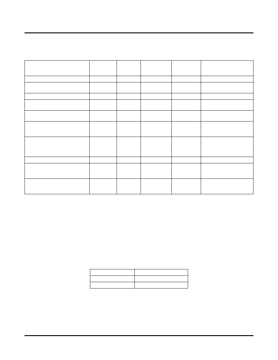
Table 15 summarizes the conditions under which the embedded core registers, SERDES, and embedded core
logic are reset under user control. The embedded core status registers are also reset on read.
Table 15. ORSO42G5 and ORSO82G5 Embedded Core Reset Conditions
SERDES Characterization Test Mode (ORSO82G5 Only)
The SERDES characterization mode is a test mode that allows for direct control and observation of the transmit
and receive SERDES interfaces at chip ports. With these modes the SERDES logic and I/O can be tested one
channel at a time in either the receive or transmit modes. The SERDES characterization mode is available for only
one block (block B) of the ORSO82G5.
The characterization test mode is congured by setting bits in the control registers via the system bus. There are
four bits that set up the test mode. The transmit characterization test mode is entered when SCHAR_ENA=1 and
SCHAR_TXSEL=1. Entering this mode will cause chip port inputs to directly control the SERDES low-speed trans-
mit ports of one of the channels as shown in Table 16.
Table 16. SERDES Transmit Characterization Mode
The x in the table will be a single channel in SERDES quad B, selected by the SCHAR_CHAN control bits. The
decoding of SCHAR_CHAN is shown in Table 17.
Reset Signal
Data Paths
Control
and Status
Registers
TCK156[A:B]
TCK78[A:B]
TCK39[A:B]
RCK78[A:B]
RWCKxx
Notes
Power up
Reset
Power on reset
PASB_RESETN pin = 0
(Hard Reset)
Reset
External input pin
FPGA Conguration
Reset
DONE pin = 0
Partial FPGA Reconguration
(with option disable TRI_IO)
—
DONE pin = 0
Internal Signal FPGA_RESET = 1
Reset
—
FPGA_RESET is FPGA
sourced
FPGA GSRN signal = 0
Optional
—
Optional
—
GSRN is FPGA sourced.
Set GSRN_DISABLE = 1
to disable this reset
SOFT_RESET = 0, 1, 0
(System Bus register based)
Reset
—
Reset
—
write SOFT_RESET = 1
(ON) then
write SOFT_RESET = 0
(OFF)
TS_ALL Pin = 1
—
External input pin
SWRST_xx= 0,1,0
xx = [AC, AD, BA, BD] or
[AA,...,BD]
Selected
channel reset
—
Selected
channel reset
Selected
channel reset
Per channel software reset
(Not self-clearing, must be
manually set and cleared.)
GSWRST_[A:B] = 0,1,0
Selected
block reset
—
Selected
block reset
Selected
block reset
Per block software reset
(Not self-clearing, must be
manually set and cleared.)
Chip Port
SERDES Input
PSCHAR_CKIO0
TBCBx
PSCHAR_LDIO[9:0]
LDINBx[9:0]
相关PDF资料 |
PDF描述 |
|---|---|
| ORSO42G5-1BMN484C | IC TRANCEIVERS FPSC 680FPGAM |
| VE-B03-IX-F1 | CONVERTER MOD DC/DC 24V 75W |
| MS27467T25A61PA | CONN PLUG 61POS STRAIGHT W/PINS |
| MS27467E25A61PA | CONN PLUG 61POS STRAIGHT W/PINS |
| MS27467E25B61PC | CONN PLUG 61POS STRAIGHT W/PINS |
相关代理商/技术参数 |
参数描述 |
|---|---|
| ORSO42G5-3BM484C | 功能描述:FPGA - 现场可编程门阵列 10368 LUT 204 I/O RoHS:否 制造商:Altera Corporation 系列:Cyclone V E 栅极数量: 逻辑块数量:943 内嵌式块RAM - EBR:1956 kbit 输入/输出端数量:128 最大工作频率:800 MHz 工作电源电压:1.1 V 最大工作温度:+ 70 C 安装风格:SMD/SMT 封装 / 箱体:FBGA-256 |
| ORSO42G5-3BMN484C | 功能描述:FPGA - 现场可编程门阵列 10368 LUT 204 I/O RoHS:否 制造商:Altera Corporation 系列:Cyclone V E 栅极数量: 逻辑块数量:943 内嵌式块RAM - EBR:1956 kbit 输入/输出端数量:128 最大工作频率:800 MHz 工作电源电压:1.1 V 最大工作温度:+ 70 C 安装风格:SMD/SMT 封装 / 箱体:FBGA-256 |
| ORSO42G5-EV | 功能描述:可编程逻辑 IC 开发工具 Eval Brd ORSO42G5 RoHS:否 制造商:Altera Corporation 产品:Development Kits 类型:FPGA 工具用于评估:5CEFA7F3 接口类型: 工作电源电压: |
| ORSO82G5 | 制造商:LATTICE 制造商全称:Lattice Semiconductor 功能描述:0.6 to 2.7 Gbps SONET Backplane Interface FPSCs |
| ORSO82G5-1BM680C | 功能描述:FPGA - 现场可编程门阵列 10368 LUT 372 I/O RoHS:否 制造商:Altera Corporation 系列:Cyclone V E 栅极数量: 逻辑块数量:943 内嵌式块RAM - EBR:1956 kbit 输入/输出端数量:128 最大工作频率:800 MHz 工作电源电压:1.1 V 最大工作温度:+ 70 C 安装风格:SMD/SMT 封装 / 箱体:FBGA-256 |
发布紧急采购,3分钟左右您将得到回复。