- 您现在的位置:买卖IC网 > PDF目录11732 > ORSO42G5-2BMN484I (Lattice Semiconductor Corporation)IC TRANCEIVERS FPSC 680FPGAM PDF资料下载
参数资料
| 型号: | ORSO42G5-2BMN484I |
| 厂商: | Lattice Semiconductor Corporation |
| 文件页数: | 145/153页 |
| 文件大小: | 0K |
| 描述: | IC TRANCEIVERS FPSC 680FPGAM |
| 产品变化通告: | Product Discontinuation 01/Aug/2011 |
| 标准包装: | 60 |
| 系列: | * |
第1页第2页第3页第4页第5页第6页第7页第8页第9页第10页第11页第12页第13页第14页第15页第16页第17页第18页第19页第20页第21页第22页第23页第24页第25页第26页第27页第28页第29页第30页第31页第32页第33页第34页第35页第36页第37页第38页第39页第40页第41页第42页第43页第44页第45页第46页第47页第48页第49页第50页第51页第52页第53页第54页第55页第56页第57页第58页第59页第60页第61页第62页第63页第64页第65页第66页第67页第68页第69页第70页第71页第72页第73页第74页第75页第76页第77页第78页第79页第80页第81页第82页第83页第84页第85页第86页第87页第88页第89页第90页第91页第92页第93页第94页第95页第96页第97页第98页第99页第100页第101页第102页第103页第104页第105页第106页第107页第108页第109页第110页第111页第112页第113页第114页第115页第116页第117页第118页第119页第120页第121页第122页第123页第124页第125页第126页第127页第128页第129页第130页第131页第132页第133页第134页第135页第136页第137页第138页第139页第140页第141页第142页第143页第144页当前第145页第146页第147页第148页第149页第150页第151页第152页第153页
Lattice Semiconductor
ORCA ORSO42G5 and ORSO82G5 Data Sheet
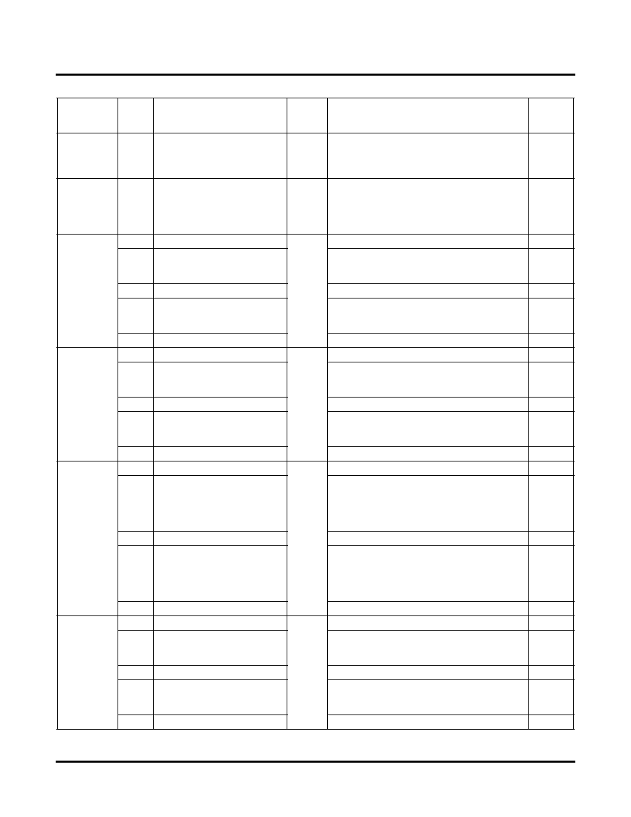
91
30A09
[0:7]
B1_ERR_CNT
00
Error counter that increments when a section
B1 error is detected on a link. The link is
selected using ERRCNT_CHSEL. This counter
is cleared on read.
Both
30A0A
[0:7]
CELL_BIP_ERR_CNT
00
Cell BIP Error Counter, Error counter that incre-
ments when a Cell BIP error is detected on a
link. The link being monitored is selected using
ERRCNT_CHSEL. This counter is cleared on
read.
Cell
30A0B
[0:2]
RSVD
00
Reserved
[3]
CELL_DRP_B2
Cell Drop, CELL_DRP_B2 = 1 indicates that a
cell has been dropped from the link group BC
and BD
Cell
[4]
RSVD
Reserved
—
[5]
CELL_DRP_A2
Cell Drop, CELL_DRP_A2 = 1 indicates that a
cell has been dropped from the link group AC
and AD
Cell
[6:7]
RSVD
Reserved
—
30A0C
[0:1]
RSVD
00
Reserved
[2]
SYNC2_B2_OOS
SYNC2_B2_OOS = 1 indicates that channels
cannot be aligned within the links BC and BD in
SONET mode
SONET
[3:4]
RSVD
Reserved
—
[5]
SYNC2_A2_OOS
SYNC2_A2_OOS = 1 indicates that channels
cannot be aligned within the AC and AD links in
SONET mode
SONET
[6:7]
SYNC2_A1_OOS
Reserved
—
30A0D
[0:1]
RSVD
00
Reserved
—
[2]
SYNC2_B2_OVFL
SYNC2_B2_OVFL = 1 indicates that the align-
ment FIFO(s) in the links BC and BD are near
overow (i.e., at the time of writing into address
0, the read address was less than
RX_FIFO_MIN)
SONET
[3:4]
RSVD
Reserved
—
[5]
SYNC2_A2_OVFL
SYNC2_A2_OVFL = 1 indicates that the align-
ment FIFO(s) in the links AC and AD are near
overow (i.e., at the time of writing into address
0, the read address was less than
RX_FIFO_MIN)
SONET
[6:7]
RSVD
Reserved
—
30A0E
[0:2]
RSVD
00
Reserved
[3]
BDL_ALIGN_ERR_B2
Alignment Error, BDL_ALIGN_ERR = 1 indi-
cates that an alignment error has occurred in
the link group pairs BC and BD
Cell
[4]
RSVD
Reserved
—
[5]
BDL_ALIGN_ERR_A2
Alignment Error, BDL_ALIGN_ERR = 1 indi-
cates that an alignment error has occurred in
the link group pairs AC and AD
Cell
[6:7]
RSVD
Reserved
—
Table 28. Common Control Register Descriptions – ORSO42G5 (Continued)
(0x)
Absolute
Address
Bit
Name
Reset
Value
(0x)
Description
Mode
相关PDF资料 |
PDF描述 |
|---|---|
| ORSO42G5-1BMN484C | IC TRANCEIVERS FPSC 680FPGAM |
| VE-B03-IX-F1 | CONVERTER MOD DC/DC 24V 75W |
| MS27467T25A61PA | CONN PLUG 61POS STRAIGHT W/PINS |
| MS27467E25A61PA | CONN PLUG 61POS STRAIGHT W/PINS |
| MS27467E25B61PC | CONN PLUG 61POS STRAIGHT W/PINS |
相关代理商/技术参数 |
参数描述 |
|---|---|
| ORSO42G5-3BM484C | 功能描述:FPGA - 现场可编程门阵列 10368 LUT 204 I/O RoHS:否 制造商:Altera Corporation 系列:Cyclone V E 栅极数量: 逻辑块数量:943 内嵌式块RAM - EBR:1956 kbit 输入/输出端数量:128 最大工作频率:800 MHz 工作电源电压:1.1 V 最大工作温度:+ 70 C 安装风格:SMD/SMT 封装 / 箱体:FBGA-256 |
| ORSO42G5-3BMN484C | 功能描述:FPGA - 现场可编程门阵列 10368 LUT 204 I/O RoHS:否 制造商:Altera Corporation 系列:Cyclone V E 栅极数量: 逻辑块数量:943 内嵌式块RAM - EBR:1956 kbit 输入/输出端数量:128 最大工作频率:800 MHz 工作电源电压:1.1 V 最大工作温度:+ 70 C 安装风格:SMD/SMT 封装 / 箱体:FBGA-256 |
| ORSO42G5-EV | 功能描述:可编程逻辑 IC 开发工具 Eval Brd ORSO42G5 RoHS:否 制造商:Altera Corporation 产品:Development Kits 类型:FPGA 工具用于评估:5CEFA7F3 接口类型: 工作电源电压: |
| ORSO82G5 | 制造商:LATTICE 制造商全称:Lattice Semiconductor 功能描述:0.6 to 2.7 Gbps SONET Backplane Interface FPSCs |
| ORSO82G5-1BM680C | 功能描述:FPGA - 现场可编程门阵列 10368 LUT 372 I/O RoHS:否 制造商:Altera Corporation 系列:Cyclone V E 栅极数量: 逻辑块数量:943 内嵌式块RAM - EBR:1956 kbit 输入/输出端数量:128 最大工作频率:800 MHz 工作电源电压:1.1 V 最大工作温度:+ 70 C 安装风格:SMD/SMT 封装 / 箱体:FBGA-256 |
发布紧急采购,3分钟左右您将得到回复。