- 您现在的位置:买卖IC网 > PDF目录11732 > ORSO42G5-2BMN484I (Lattice Semiconductor Corporation)IC TRANCEIVERS FPSC 680FPGAM PDF资料下载
参数资料
| 型号: | ORSO42G5-2BMN484I |
| 厂商: | Lattice Semiconductor Corporation |
| 文件页数: | 141/153页 |
| 文件大小: | 0K |
| 描述: | IC TRANCEIVERS FPSC 680FPGAM |
| 产品变化通告: | Product Discontinuation 01/Aug/2011 |
| 标准包装: | 60 |
| 系列: | * |
第1页第2页第3页第4页第5页第6页第7页第8页第9页第10页第11页第12页第13页第14页第15页第16页第17页第18页第19页第20页第21页第22页第23页第24页第25页第26页第27页第28页第29页第30页第31页第32页第33页第34页第35页第36页第37页第38页第39页第40页第41页第42页第43页第44页第45页第46页第47页第48页第49页第50页第51页第52页第53页第54页第55页第56页第57页第58页第59页第60页第61页第62页第63页第64页第65页第66页第67页第68页第69页第70页第71页第72页第73页第74页第75页第76页第77页第78页第79页第80页第81页第82页第83页第84页第85页第86页第87页第88页第89页第90页第91页第92页第93页第94页第95页第96页第97页第98页第99页第100页第101页第102页第103页第104页第105页第106页第107页第108页第109页第110页第111页第112页第113页第114页第115页第116页第117页第118页第119页第120页第121页第122页第123页第124页第125页第126页第127页第128页第129页第130页第131页第132页第133页第134页第135页第136页第137页第138页第139页第140页当前第141页第142页第143页第144页第145页第146页第147页第148页第149页第150页第151页第152页第153页
Lattice Semiconductor
ORCA ORSO42G5 and ORSO82G5 Data Sheet
88
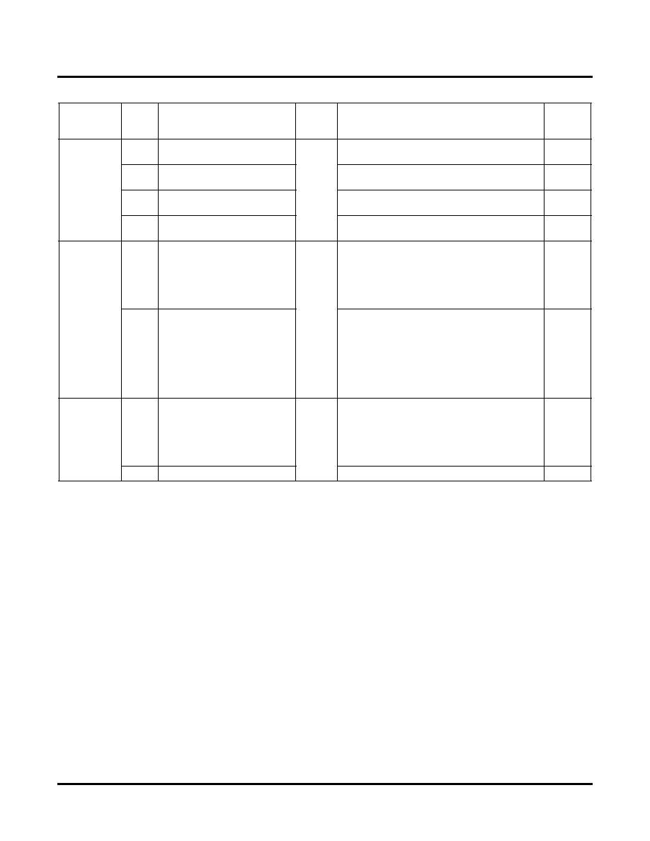
Table 28. Common Control Register Descriptions – ORSO42G5
(0x)
Absolute
Address
Bit
Name
Reset
Value
(0x)
Description
Mode
30A00
[0:1]
RCKSELB
00
“10” - Channel BC source for clock RCK78B
“11” - Channel BD source for clock RCK78B
Both
[2:3]
TCKSELB
“10” - Channel BC source for clock TCK78B
“11” - Channel BD source for clock TCK78B
Both
[4:5]
RCKSELA
“10” - Channel AC source for clock RCK78A
“11” - Channel AD source for clock RCK78A
Both
[6:7]
TCKSELA
“10” - Channel AC source for clock TCK78A
“11” - Channel AD source for clock TCK78A
Both
30A01
[0:2]
CELL_SIZE
00
Cell Size, Three bits to set cell size.
“000” - Cell size is 75 bytes,
“001” - Cell size is 79 bytes,
“010” - Cell size is 83 bytes,
“011” - Cell size is 91 bytes
These are the only supported cell sizes.
Cell
[3:7]
RX_FIFO_MIN
Set Minimum threshold value for alignment
FIFO in SONET mode. When the read address
for the FIFO is below this value at the time when
write address is zero, it indicates that the FIFO
is near overow. This event will go high only
once during a frame when a framing byte has
been detected by the aligner. The default
threshold value is “00000”.
SONET
30A02
0
TX_DISABLE_ON_RDI
00
Transmitter Disable on RDI (Detection), If
TX_DISABLE_ON_RDI = 1 - No cell data is
transmitted on a link in which a RDI has been
detected by the corresponding link’s receiver. If
this bit is set to 0, cell data will be transmitted on
a link irrespective of detection of a RDI.
Cell
[1:7]
RSVD
Reserved
—
相关PDF资料 |
PDF描述 |
|---|---|
| ORSO42G5-1BMN484C | IC TRANCEIVERS FPSC 680FPGAM |
| VE-B03-IX-F1 | CONVERTER MOD DC/DC 24V 75W |
| MS27467T25A61PA | CONN PLUG 61POS STRAIGHT W/PINS |
| MS27467E25A61PA | CONN PLUG 61POS STRAIGHT W/PINS |
| MS27467E25B61PC | CONN PLUG 61POS STRAIGHT W/PINS |
相关代理商/技术参数 |
参数描述 |
|---|---|
| ORSO42G5-3BM484C | 功能描述:FPGA - 现场可编程门阵列 10368 LUT 204 I/O RoHS:否 制造商:Altera Corporation 系列:Cyclone V E 栅极数量: 逻辑块数量:943 内嵌式块RAM - EBR:1956 kbit 输入/输出端数量:128 最大工作频率:800 MHz 工作电源电压:1.1 V 最大工作温度:+ 70 C 安装风格:SMD/SMT 封装 / 箱体:FBGA-256 |
| ORSO42G5-3BMN484C | 功能描述:FPGA - 现场可编程门阵列 10368 LUT 204 I/O RoHS:否 制造商:Altera Corporation 系列:Cyclone V E 栅极数量: 逻辑块数量:943 内嵌式块RAM - EBR:1956 kbit 输入/输出端数量:128 最大工作频率:800 MHz 工作电源电压:1.1 V 最大工作温度:+ 70 C 安装风格:SMD/SMT 封装 / 箱体:FBGA-256 |
| ORSO42G5-EV | 功能描述:可编程逻辑 IC 开发工具 Eval Brd ORSO42G5 RoHS:否 制造商:Altera Corporation 产品:Development Kits 类型:FPGA 工具用于评估:5CEFA7F3 接口类型: 工作电源电压: |
| ORSO82G5 | 制造商:LATTICE 制造商全称:Lattice Semiconductor 功能描述:0.6 to 2.7 Gbps SONET Backplane Interface FPSCs |
| ORSO82G5-1BM680C | 功能描述:FPGA - 现场可编程门阵列 10368 LUT 372 I/O RoHS:否 制造商:Altera Corporation 系列:Cyclone V E 栅极数量: 逻辑块数量:943 内嵌式块RAM - EBR:1956 kbit 输入/输出端数量:128 最大工作频率:800 MHz 工作电源电压:1.1 V 最大工作温度:+ 70 C 安装风格:SMD/SMT 封装 / 箱体:FBGA-256 |
发布紧急采购,3分钟左右您将得到回复。