- 您现在的位置:买卖IC网 > PDF目录17102 > ORT42G5-EV (Lattice Semiconductor Corporation)BOARD EVAL ORT42G5/CABLE/ADAPTER PDF资料下载
参数资料
| 型号: | ORT42G5-EV |
| 厂商: | Lattice Semiconductor Corporation |
| 文件页数: | 71/119页 |
| 文件大小: | 0K |
| 描述: | BOARD EVAL ORT42G5/CABLE/ADAPTER |
| 标准包装: | 1 |
| 系列: | ORCA® 4 系列 |
| 类型: | FPGA |
| 适用于相关产品: | ORT42G5 |
| 所含物品: | 板,线缆,电源 |
| 其它名称: | ORT42G5EV |
第1页第2页第3页第4页第5页第6页第7页第8页第9页第10页第11页第12页第13页第14页第15页第16页第17页第18页第19页第20页第21页第22页第23页第24页第25页第26页第27页第28页第29页第30页第31页第32页第33页第34页第35页第36页第37页第38页第39页第40页第41页第42页第43页第44页第45页第46页第47页第48页第49页第50页第51页第52页第53页第54页第55页第56页第57页第58页第59页第60页第61页第62页第63页第64页第65页第66页第67页第68页第69页第70页当前第71页第72页第73页第74页第75页第76页第77页第78页第79页第80页第81页第82页第83页第84页第85页第86页第87页第88页第89页第90页第91页第92页第93页第94页第95页第96页第97页第98页第99页第100页第101页第102页第103页第104页第105页第106页第107页第108页第109页第110页第111页第112页第113页第114页第115页第116页第117页第118页第119页
Lattice Semiconductor
ORCA ORT42G5 and ORT82G5 Data Sheet
55
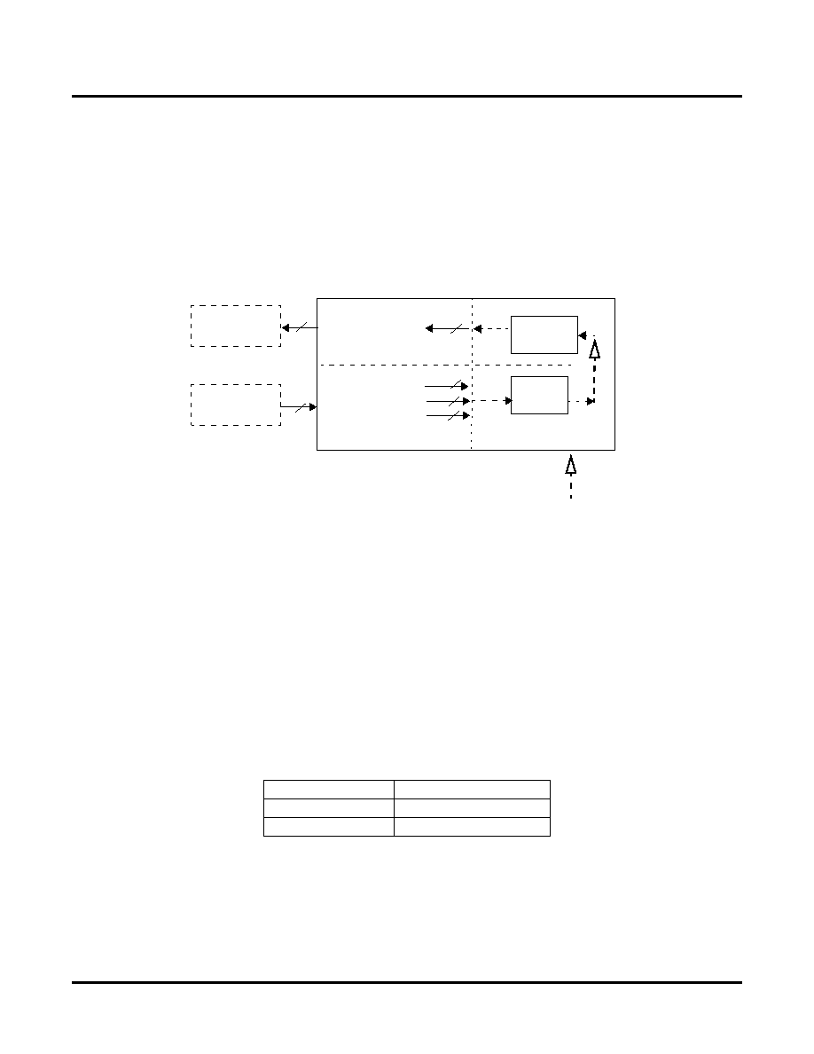
Parallel Loopback at MUX/DEMUX Boundary, Excluding SERDES
This is a low-frequency test mode used to test the MUX/DEMUX logic block. As with the mode described in the pre-
vious section, the loopback path is at the interface between the SERDES blocks and the MUX and DEMUX blocks
and uses the parallel 10-bit buses at these interfaces (see Figure 33). However, the loopback connection is made
such that the output signals from the TX MUX block are used as the input signals to the RX SERDES block. In this
loopback mode the MRWDxx[39:0], TWDxx[31:0], TCOMMAxx[3:0] and TBIT9xx[3:0] signal lines function normally
and the high-speed serial input and output buffers are not used. Use of this mode also requires conguration of the
FPGA logic to connect the MRWDxx[39:0], TWDxx[31:0], TCOMMAxx[3:0] and TBIT9xx[3:0] signal lines to exter-
nal pins. The basic loopback path is shown in Figure 33.
Figure 33. Parallel Loopback at MUX/DEMUX Boundary, Excluding SERDES
This test mode is enabled by setting the pin PLOOP_TEST_ENN to 0. PASB_TESTCLK must be running in this
mode at 4x frequency of RSYS_CLK[A2, B2] or TSYS_CLK_[AC, AD, BC, BD] for the ORT42G5 and
RSYS_CLK[A1,A2,B1,B2] or TSYS_CLK_[AA, AB... BD] for the ORT82G5.
SERDES Characterization Test Mode (ORT82G5 Only)
The SERDES characterization mode is a test mode that allows for direct control and observation of the transmit
and receive SERDES interfaces at chip ports. With these modes the SERDES logic and I/O can be tested one
channel at a time in either the receive or transmit modes. The SERDES characterization mode is available for only
one quad (quad B) of the ORT82G5.
The characterization test mode is congured by setting bits in the control registers via the system bus. There are
four bits that set up the test mode. The transmit characterization test mode is entered when SCHAR_ENA=1 and
SCHAR_TXSEL=1. Entering this mode will cause chip port inputs to directly control the SERDES low-speed trans-
mit ports of one of the channels as shown in Table 23.
Table 23. SERDES Transmit Characterization Mode
The x in the table will be a single channel in SERDES quad B, selected by the SCHAR_CHAN control bits. The
decoding of SCHAR_CHAN is shown in Table 24.
Chip Port
SERDES Input
PSCHAR_CKIO0
TBCBx
PSCHAR_LDIO[9:0]
LDINBx[9:0]
DEMUX
MUX
Embedded Core
FPGA Logic
40
MRWDxx[39:0]
32
4
Receive
Transmit
TWDxx[31:0]
TCOMMAxx[3:0]
TBIT9xx[3:0]
Data
Checking
Data
Generation
n
m
{
Parallel
Loopback
Connection
Test
Equipment
相关PDF资料 |
PDF描述 |
|---|---|
| REF194GS-REEL | IC VREF SERIES PREC 4.5V 8-SOIC |
| ECC24DCMT | CONN EDGECARD 48POS .100 WW |
| ORSO42G5-EV | BOARD EVAL DEV PLATFORM ORSO42G5 |
| EEM22DTAT-S189 | CONN EDGECARD 44POS R/A .156 SLD |
| ECC20DRES | CONN EDGECARD 40POS .100 EYELET |
相关代理商/技术参数 |
参数描述 |
|---|---|
| ORT43S | 制造商:BOT 制造商全称:Bedford Opto Technology Ltd. 功能描述:3mm LED CIRCUIT BOARD INDICATOR 4 TIER SHROUDED |
| ORT43SBCBCBCBC | 制造商:BOT 制造商全称:Bedford Opto Technology Ltd. 功能描述:3mm LED CIRCUIT BOARD INDICATOR 4 TIER SHROUDED |
| ORT43SBCBCBCG | 制造商:BOT 制造商全称:Bedford Opto Technology Ltd. 功能描述:3mm LED CIRCUIT BOARD INDICATOR 4 TIER SHROUDED |
| ORT43SBCBCBCO | 制造商:BOT 制造商全称:Bedford Opto Technology Ltd. 功能描述:3mm LED CIRCUIT BOARD INDICATOR 4 TIER SHROUDED |
| ORT43SBCBCBCR | 制造商:BOT 制造商全称:Bedford Opto Technology Ltd. 功能描述:3mm LED CIRCUIT BOARD INDICATOR 4 TIER SHROUDED |
发布紧急采购,3分钟左右您将得到回复。