- 您现在的位置:买卖IC网 > PDF目录17102 > ORT42G5-EV (Lattice Semiconductor Corporation)BOARD EVAL ORT42G5/CABLE/ADAPTER PDF资料下载
参数资料
| 型号: | ORT42G5-EV |
| 厂商: | Lattice Semiconductor Corporation |
| 文件页数: | 99/119页 |
| 文件大小: | 0K |
| 描述: | BOARD EVAL ORT42G5/CABLE/ADAPTER |
| 标准包装: | 1 |
| 系列: | ORCA® 4 系列 |
| 类型: | FPGA |
| 适用于相关产品: | ORT42G5 |
| 所含物品: | 板,线缆,电源 |
| 其它名称: | ORT42G5EV |
第1页第2页第3页第4页第5页第6页第7页第8页第9页第10页第11页第12页第13页第14页第15页第16页第17页第18页第19页第20页第21页第22页第23页第24页第25页第26页第27页第28页第29页第30页第31页第32页第33页第34页第35页第36页第37页第38页第39页第40页第41页第42页第43页第44页第45页第46页第47页第48页第49页第50页第51页第52页第53页第54页第55页第56页第57页第58页第59页第60页第61页第62页第63页第64页第65页第66页第67页第68页第69页第70页第71页第72页第73页第74页第75页第76页第77页第78页第79页第80页第81页第82页第83页第84页第85页第86页第87页第88页第89页第90页第91页第92页第93页第94页第95页第96页第97页第98页当前第99页第100页第101页第102页第103页第104页第105页第106页第107页第108页第109页第110页第111页第112页第113页第114页第115页第116页第117页第118页第119页
Lattice Semiconductor
ORCA ORT42G5 and ORT82G5 Data Sheet
80
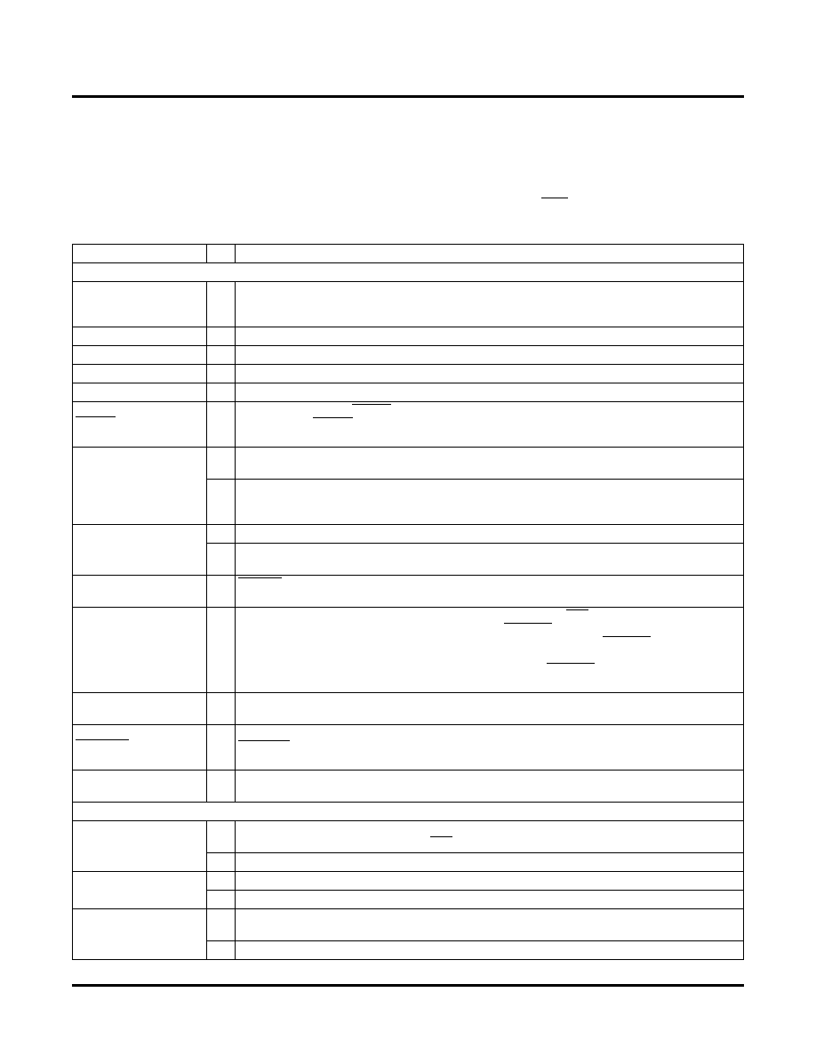
Pin Descriptions
This section describes the pins found on the Series 4 FPGAs. Any pin not described in this table is a user-program-
mable I/O. During conguration, the user-programmable I/Os are 3-stated with an internal pull-up resistor. If any pin
is not used (or not bonded to a package pin), it is also 3-stated with an internal pull-up resistor after conguration.
The pin descriptions in Table and throughout this data sheet show active-low signals with an overscore. The pack-
age pinout tables that follow, show this as a signal ending with _N. For example LDC and LDC_N are equivalent.
Table 40. Pin Descriptions
Symbol
I/O
Description
Dedicated Pins
VDD33
— 3.3V positive power supply. This power supply is used for 3.3V conguration RAMs and internal
PLLs. When using PLLs, this power supply should be well isolated from all other power supplies
on the board for proper operation.
VDD
15
— 1.5V positive power supply for internal logic.
VDDIO
— Positive power supply used by I/O banks.
VSS
— Ground.
PTEMP
I
Temperature sensing diode pin. Dedicated input.
RESET
I
During conguration, RESET forces the restart of conguration and a pull-up is enabled. After
conguration, RESET can be used as a general FPGA input or as a direct input, which causes
all PLC latches/FFs to be asynchronously set/reset.
CCLK
O
In the master and asynchronous peripheral modes, CCLK is an output which strobes congura-
tion data in.
I
In the slave or readback after conguration, CCLK is input synchronous with the data on DIN or
D[7:0]. CCLK is an output for daisy-chain operation when the lead device is in master, periph-
eral, or system bus modes.
DONE
I
As an input, a low level on DONE delays FPGA start-up after conguration.
1
O
As an active-high, open-drain output, a high level on this signal indicates that conguration is
complete. DONE has an optional pull-up resistor.
PRGRM
I
PRGRM
is an active-low input that forces the restart of conguration and resets the boundary-
scan circuitry. This pin always has an active pull-up.
RD_CFG
I
This pin must be held high during device initialization until the INIT pin goes high. This pin
always has an active pull-up. During conguration, RD_CFG is an active-low input that activates
the TS_ALL function and 3-states all of the I/O.
After conguration, RD_CFG can be selected
(via a bit stream option) to activate the TS_ALL function as described above, or, if readback is
enabled via a bit stream option, a high-to-low transition on RD_CFG will initiate readback of the
conguration data, including PFU output states, starting with frame address 0.
RD_DATA/TDO
O
RD_DATA/TDO is a dual-function pin. If used for readback, RD_DATA provides conguration
data out. If used in boundary-scan, TDO is test data out.
CFG_IRQ/MPI_IRQ
O
During JTAG, slave, master, and asynchronous peripheral conguration assertion on this
CFG_IRQ
(active-low) indicates an error or errors for block RAM or FPSC initialization.
MPI
active-low interrupt request output, when the MPI is used.
LVDS_R
— Reference resistor connection for controlled impedance termination of Series 4 FPGA LVDS
inputs.
Special-Purpose Pins
M[3:0]
I
During powerup and initialization, M0—M3 are used to select the conguration mode with their
values latched on the rising edge of INIT. During conguration, a pull-up is enabled.
I/O After conguration, these pins are user-programmable I/O.
1
PLL_CK[0:7][TC]
I
Semi-dedicated PLL clock pins. During conguration they are 3-stated with a pull up.
I/O These pins are user-programmable I/O pins if not used by PLLs after conguration.
P[TBLR]CLK[1:0][TC]
I
Pins dedicated for the primary clock. Input pins on the middle of each side with differential pair-
ing.
I/O After conguration these pins are user programmable I/O, if not used for clock inputs.
相关PDF资料 |
PDF描述 |
|---|---|
| REF194GS-REEL | IC VREF SERIES PREC 4.5V 8-SOIC |
| ECC24DCMT | CONN EDGECARD 48POS .100 WW |
| ORSO42G5-EV | BOARD EVAL DEV PLATFORM ORSO42G5 |
| EEM22DTAT-S189 | CONN EDGECARD 44POS R/A .156 SLD |
| ECC20DRES | CONN EDGECARD 40POS .100 EYELET |
相关代理商/技术参数 |
参数描述 |
|---|---|
| ORT43S | 制造商:BOT 制造商全称:Bedford Opto Technology Ltd. 功能描述:3mm LED CIRCUIT BOARD INDICATOR 4 TIER SHROUDED |
| ORT43SBCBCBCBC | 制造商:BOT 制造商全称:Bedford Opto Technology Ltd. 功能描述:3mm LED CIRCUIT BOARD INDICATOR 4 TIER SHROUDED |
| ORT43SBCBCBCG | 制造商:BOT 制造商全称:Bedford Opto Technology Ltd. 功能描述:3mm LED CIRCUIT BOARD INDICATOR 4 TIER SHROUDED |
| ORT43SBCBCBCO | 制造商:BOT 制造商全称:Bedford Opto Technology Ltd. 功能描述:3mm LED CIRCUIT BOARD INDICATOR 4 TIER SHROUDED |
| ORT43SBCBCBCR | 制造商:BOT 制造商全称:Bedford Opto Technology Ltd. 功能描述:3mm LED CIRCUIT BOARD INDICATOR 4 TIER SHROUDED |
发布紧急采购,3分钟左右您将得到回复。