- 您现在的位置:买卖IC网 > PDF目录1959 > P89LPC954FBD44,151 (NXP Semiconductors)IC 80C51 MCU FLASH 16K 44LQFP PDF资料下载
参数资料
| 型号: | P89LPC954FBD44,151 |
| 厂商: | NXP Semiconductors |
| 文件页数: | 2/69页 |
| 文件大小: | 0K |
| 描述: | IC 80C51 MCU FLASH 16K 44LQFP |
| 标准包装: | 160 |
| 系列: | LPC900 |
| 核心处理器: | 8051 |
| 芯体尺寸: | 8-位 |
| 速度: | 18MHz |
| 连通性: | I²C,SPI,UART/USART |
| 外围设备: | 欠压检测/复位,POR,PWM,WDT |
| 输入/输出数: | 40 |
| 程序存储器容量: | 16KB(16K x 8) |
| 程序存储器类型: | 闪存 |
| RAM 容量: | 512 x 8 |
| 电压 - 电源 (Vcc/Vdd): | 2.4 V ~ 3.6 V |
| 数据转换器: | A/D 8x10b |
| 振荡器型: | 内部 |
| 工作温度: | -40°C ~ 85°C |
| 封装/外壳: | 44-LQFP |
| 包装: | 托盘 |
| 配用: | 568-1759-ND - EMULATOR DEBUGGER/PROGRMMR LPC9X |
| 其它名称: | 568-7917 568-7917-ND 568-8269 935284303151 P89LPC954FBD44,151-ND P89LPC954FBD44-S P89LPC954FBD44-S-ND |
第1页当前第2页第3页第4页第5页第6页第7页第8页第9页第10页第11页第12页第13页第14页第15页第16页第17页第18页第19页第20页第21页第22页第23页第24页第25页第26页第27页第28页第29页第30页第31页第32页第33页第34页第35页第36页第37页第38页第39页第40页第41页第42页第43页第44页第45页第46页第47页第48页第49页第50页第51页第52页第53页第54页第55页第56页第57页第58页第59页第60页第61页第62页第63页第64页第65页第66页第67页第68页第69页
P89LPC952_954_4
NXP B.V. 2008. All rights reserved.
Product data sheet
Rev. 04 — 24 July 2008
10 of 69
NXP Semiconductors
P89LPC952/954
8-bit microcontroller with 10-bit ADC
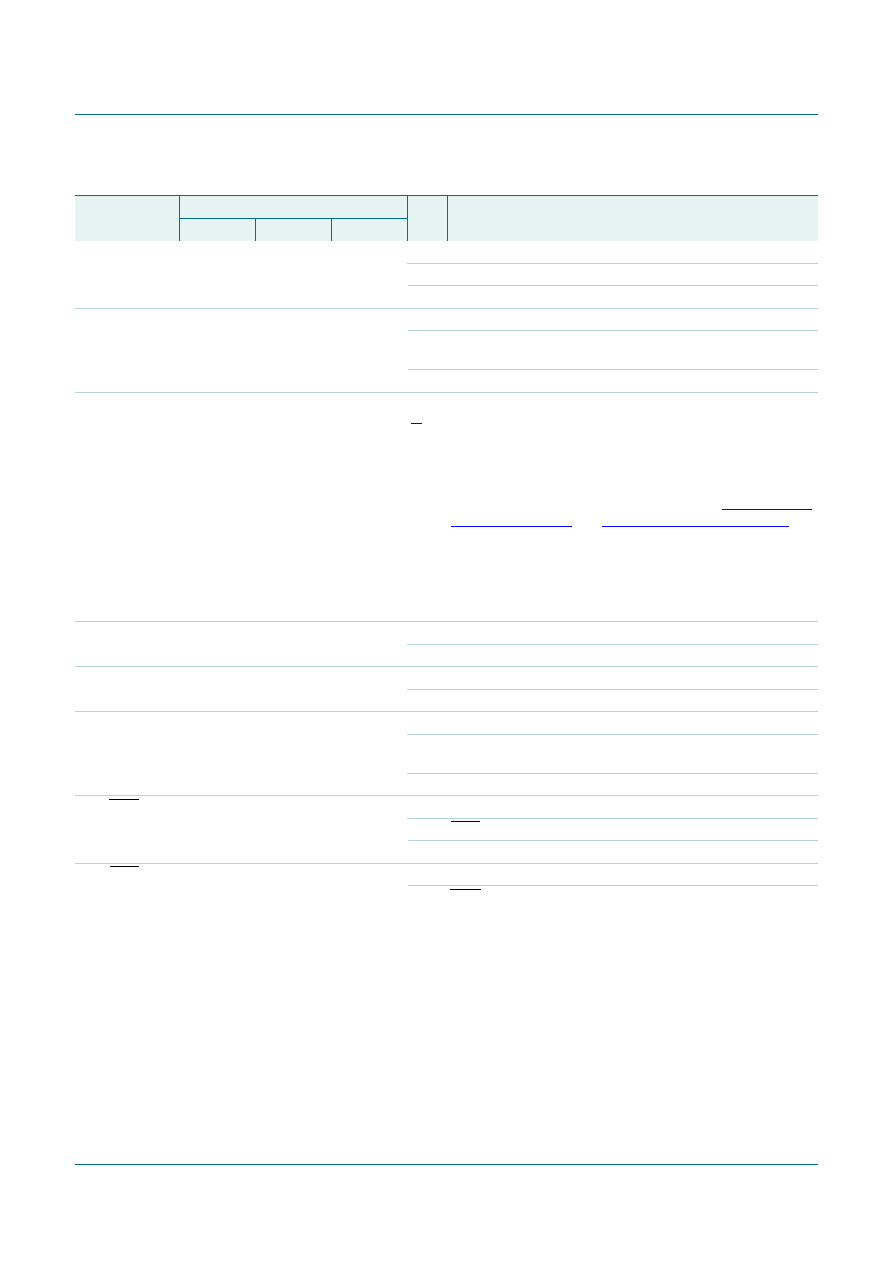
P0.6/CMP1/
KBI6
34
37
31
I/O
P0.6 — Port 0 bit 6.
O
CMP1 — Comparator 1 output.
I
KBI6 — Keyboard input 6.
P0.7/T1/KBI7
31
35
29
I/O
P0.7 — Port 0 bit 7.
I/O
T1 — Timer/counter 1 external count input or overow
output.
I
KBI7 — Keyboard input 7.
P1.0 to P1.7
I/O, I
Port 1: Port 1 is an 8-bit I/O port with a user-congurable
output type, except for three pins as noted below. During
reset Port 1 latches are congured in the input only mode
with the internal pull-up disabled. The operation of the
congurable Port 1 pins as inputs and outputs depends upon
the port conguration selected. Each of the congurable port
pins are programmed independently. Refer to Section 7.13.1
details. P1.2 to P1.3 are open drain when used as outputs.
P1.5 is input only.
All pins have Schmitt triggered inputs.
Port 1 also provides various special functions as described
below:
P1.0/TXD0
4
10
4
I/O
P1.0 — Port 1 bit 0.
O
TXD0 — Transmitter output for serial port 0.
P1.1/RXD0
3
9
3
I/O
P1.1 — Port 1 bit 1.
I
RXD0 — Receiver input for serial port 0.
P1.2/T0/SCL
2
8
2
I/O
P1.2 — Port 1 bit 2 (open-drain when used as output).
I/O
T0 — Timer/counter 0 external count input or overow
output (open-drain when used as output).
I/O
SCL — I2C-bus serial clock input/output.
P1.3/INT0/SDA
1
7
1
I/O
P1.3 — Port 1 bit 3 (open-drain when used as output).
I
INT0 — External interrupt 0 input.
I/O
SDA — I2C-bus serial data input/output.
P1.4/INT1
48
6
44
I/O
P1.4 — Port 1 bit 4.
I
INT1 — External interrupt 1 input.
Table 3.
Pin description …continued
Symbol
Pin
Type Description
LQFP48
PLCC44
LQFP44
相关PDF资料 |
PDF描述 |
|---|---|
| P89LPC972FN,129 | MCU 80C51 8KB FLASH 20DIP |
| P89LPC985FDH,529 | IC 80C51 MCU KB FLASH 28TSSOP |
| P89V51RC2FA,512 | IC 80C51 MCU FLASH 32K 44-PLCC |
| P89V52X2FN,112 | IC 80C51 MCU FLASH 8K 40-DIP |
| P89V662FA,512 | IC 80C51 MCU FLASH 32K 44-PLCC |
相关代理商/技术参数 |
参数描述 |
|---|---|
| P89LPC954FBD44-S | 功能描述:8位微控制器 -MCU 16K FL/1K RAM/512B EE/10B ADC RoHS:否 制造商:Silicon Labs 核心:8051 处理器系列:C8051F39x 数据总线宽度:8 bit 最大时钟频率:50 MHz 程序存储器大小:16 KB 数据 RAM 大小:1 KB 片上 ADC:Yes 工作电源电压:1.8 V to 3.6 V 工作温度范围:- 40 C to + 105 C 封装 / 箱体:QFN-20 安装风格:SMD/SMT |
| P89LPC954FBD48 | 制造商:PHILIPS 制造商全称:NXP Semiconductors 功能描述:8-bit microcontroller with accelerated two-clock 80C51 core 8 kB/16 kB 3 V byte-erasable flash with 10-bit ADC |
| P89LPC954FBD48,151 | 功能描述:8位微控制器 -MCU 8B MCU 2-CLOCK 80C51 8/16KB 3V 10B RoHS:否 制造商:Silicon Labs 核心:8051 处理器系列:C8051F39x 数据总线宽度:8 bit 最大时钟频率:50 MHz 程序存储器大小:16 KB 数据 RAM 大小:1 KB 片上 ADC:Yes 工作电源电压:1.8 V to 3.6 V 工作温度范围:- 40 C to + 105 C 封装 / 箱体:QFN-20 安装风格:SMD/SMT |
| P89LPC970 | 制造商:PHILIPS 制造商全称:NXP Semiconductors 功能描述:8-bit microcontroller with accelerated two-clock 80C51 core 2 kB/4 kB/8 kB wide-voltage byte-erasable flash |
| P89LPC970FDH | 制造商:PHILIPS 制造商全称:NXP Semiconductors 功能描述:8-bit microcontroller with accelerated two-clock 80C51 core 2 kB/4 kB/8 kB wide-voltage byte-erasable flash |
发布紧急采购,3分钟左右您将得到回复。