- 您现在的位置:买卖IC网 > PDF目录17011 > PCM18XK1 (Microchip Technology)MODULE PROC PIC18F8680,6680,8565 PDF资料下载
参数资料
| 型号: | PCM18XK1 |
| 厂商: | Microchip Technology |
| 文件页数: | 224/424页 |
| 文件大小: | 0K |
| 描述: | MODULE PROC PIC18F8680,6680,8565 |
| 标准包装: | 1 |
| 附件类型: | 处理器模块 |
| 适用于相关产品: | ICE2000 |
| 产品目录页面: | 658 (CN2011-ZH PDF) |
| 配用: | ICE2000-ND - EMULATOR MPLAB-ICE 2000 POD |
| 相关产品: | DVA18PQ802-ND - DEVICE ATP FOR ICE2000 |
第1页第2页第3页第4页第5页第6页第7页第8页第9页第10页第11页第12页第13页第14页第15页第16页第17页第18页第19页第20页第21页第22页第23页第24页第25页第26页第27页第28页第29页第30页第31页第32页第33页第34页第35页第36页第37页第38页第39页第40页第41页第42页第43页第44页第45页第46页第47页第48页第49页第50页第51页第52页第53页第54页第55页第56页第57页第58页第59页第60页第61页第62页第63页第64页第65页第66页第67页第68页第69页第70页第71页第72页第73页第74页第75页第76页第77页第78页第79页第80页第81页第82页第83页第84页第85页第86页第87页第88页第89页第90页第91页第92页第93页第94页第95页第96页第97页第98页第99页第100页第101页第102页第103页第104页第105页第106页第107页第108页第109页第110页第111页第112页第113页第114页第115页第116页第117页第118页第119页第120页第121页第122页第123页第124页第125页第126页第127页第128页第129页第130页第131页第132页第133页第134页第135页第136页第137页第138页第139页第140页第141页第142页第143页第144页第145页第146页第147页第148页第149页第150页第151页第152页第153页第154页第155页第156页第157页第158页第159页第160页第161页第162页第163页第164页第165页第166页第167页第168页第169页第170页第171页第172页第173页第174页第175页第176页第177页第178页第179页第180页第181页第182页第183页第184页第185页第186页第187页第188页第189页第190页第191页第192页第193页第194页第195页第196页第197页第198页第199页第200页第201页第202页第203页第204页第205页第206页第207页第208页第209页第210页第211页第212页第213页第214页第215页第216页第217页第218页第219页第220页第221页第222页第223页当前第224页第225页第226页第227页第228页第229页第230页第231页第232页第233页第234页第235页第236页第237页第238页第239页第240页第241页第242页第243页第244页第245页第246页第247页第248页第249页第250页第251页第252页第253页第254页第255页第256页第257页第258页第259页第260页第261页第262页第263页第264页第265页第266页第267页第268页第269页第270页第271页第272页第273页第274页第275页第276页第277页第278页第279页第280页第281页第282页第283页第284页第285页第286页第287页第288页第289页第290页第291页第292页第293页第294页第295页第296页第297页第298页第299页第300页第301页第302页第303页第304页第305页第306页第307页第308页第309页第310页第311页第312页第313页第314页第315页第316页第317页第318页第319页第320页第321页第322页第323页第324页第325页第326页第327页第328页第329页第330页第331页第332页第333页第334页第335页第336页第337页第338页第339页第340页第341页第342页第343页第344页第345页第346页第347页第348页第349页第350页第351页第352页第353页第354页第355页第356页第357页第358页第359页第360页第361页第362页第363页第364页第365页第366页第367页第368页第369页第370页第371页第372页第373页第374页第375页第376页第377页第378页第379页第380页第381页第382页第383页第384页第385页第386页第387页第388页第389页第390页第391页第392页第393页第394页第395页第396页第397页第398页第399页第400页第401页第402页第403页第404页第405页第406页第407页第408页第409页第410页第411页第412页第413页第414页第415页第416页第417页第418页第419页第420页第421页第422页第423页第424页
PIC18F6585/8585/6680/8680
DS30491C-page 28
2004 Microchip Technology Inc.
2.6.2
OSCILLATOR TRANSITIONS
PIC18F6585/8585/6680/8680 devices contain circuitry
to prevent “glitches” when switching between oscillator
sources. Essentially, the circuitry waits for eight rising
edges of the clock source that the processor is switch-
ing to. This ensures that the new clock source is stable
and that its pulse width will not be less than the shortest
pulse width of the two clock sources.
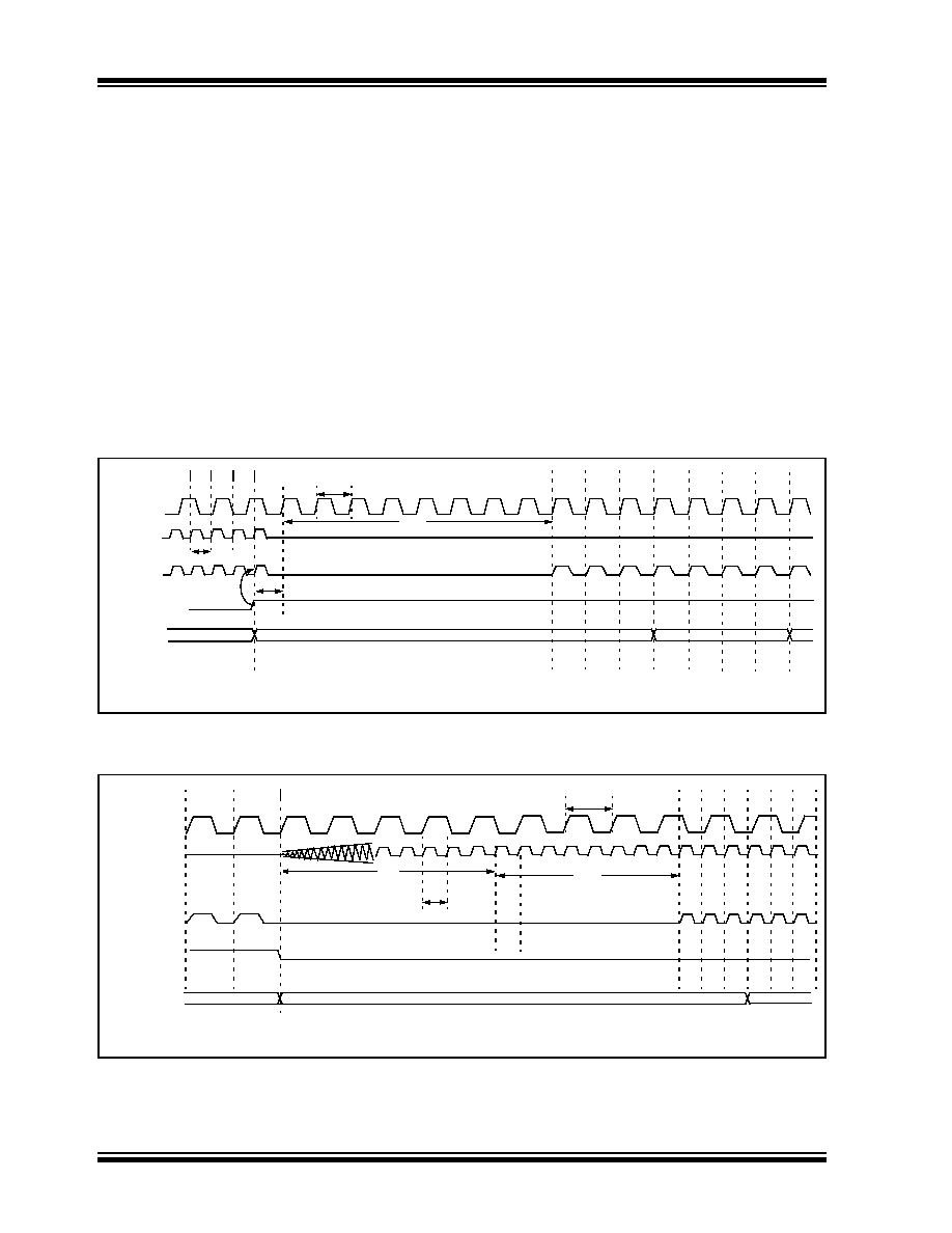
A timing diagram, indicating the transition from the
main oscillator to the Timer1 oscillator, is shown in
Figure 2-8. The Timer1 oscillator is assumed to be run-
ning all the time. After the SCS0 bit is set, the processor
is frozen at the next occurring Q1 cycle. After eight
synchronization cycles are counted from the Timer1
oscillator, operation resumes. No additional delays are
required after the synchronization cycles.
The sequence of events that takes place when switch-
ing from the Timer1 oscillator to the main oscillator will
depend on the mode of the main oscillator. In addition
to eight clock cycles of the main oscillator, additional
delays may take place.
If the main oscillator is configured for an external
crystal (HS, XT, LP), then the transition will take place
after an oscillator start-up time (TOST) has occurred. A
timing diagram, indicating the transition from the
Timer1 oscillator to the main oscillator for HS, XT and
LP modes, is shown in Figure 2-9.
FIGURE 2-8:
TIMING DIAGRAM FOR TRANSITION FROM OSC1 TO TIMER1 OSCILLATOR
FIGURE 2-9:
TIMING FOR TRANSITION BETWEEN TIMER1 AND OSC1 (HS, XT, LP)
Q3
Q2
Q1
Q4
Q3
Q2
OSC1
Internal
SCS
(OSCCON<0>)
Program
PC + 2
PC
Note:
TDLY is the delay from SCS high to first count of transition circuit.
Q1
T1OSI
Q4
Q1
PC + 4
Q1
TSCS
Clock
Counter
System
Q2
Q3
Q4
Q1
TDLY
TT1P
TOSC
2
1
3
4
5678
Q3
Q4
Q1
Q2
Q3
Q4
Q1
Q2
OSC1
Internal
SCS
(OSCCON<0>)
Program
PC
PC + 2
Note:
TOST = 1024 TOSC (drawing not to scale).
T1OSI
System Clock
TOST
Q1
PC + 6
TT1P
TOSC
TSCS
12
3
4
5
6
7
8
Counter
相关PDF资料 |
PDF描述 |
|---|---|
| 0982660125 | CBL 12POS 0.5MM JMPR TYPE A 5" |
| GBM25DCTT | CONN EDGECARD 50POS DIP .156 SLD |
| ESC05DTEH | CONN EDGECARD 10POS .100 EYELET |
| GCM22DCCN | CONN EDGECARD 44POS R/A .156 SLD |
| PCM16YN0 | MODULE PROC FOR PIC16F785 |
相关代理商/技术参数 |
参数描述 |
|---|---|
| PCM18XL0 | 功能描述:插座和适配器 Processor MOD RoHS:否 制造商:Silicon Labs 产品:Adapter 用于:EM35x |
| PCM18XM0 | 制造商:Microchip Technology Inc 功能描述:PROCESSOR MODULE |
| PCM18XN0 | 功能描述:插座和适配器 - RoHS:否 制造商:Silicon Labs 产品:Adapter 用于:EM35x |
| PCM18XN1 | 功能描述:插座和适配器 PIC18F4525 Proc Mod RoHS:否 制造商:Silicon Labs 产品:Adapter 用于:EM35x |
| PCM18XP0 | 功能描述:插座和适配器 - RoHS:否 制造商:Silicon Labs 产品:Adapter 用于:EM35x |
发布紧急采购,3分钟左右您将得到回复。