- 您现在的位置:买卖IC网 > PDF目录17011 > PCM18XK1 (Microchip Technology)MODULE PROC PIC18F8680,6680,8565 PDF资料下载
参数资料
| 型号: | PCM18XK1 |
| 厂商: | Microchip Technology |
| 文件页数: | 68/424页 |
| 文件大小: | 0K |
| 描述: | MODULE PROC PIC18F8680,6680,8565 |
| 标准包装: | 1 |
| 附件类型: | 处理器模块 |
| 适用于相关产品: | ICE2000 |
| 产品目录页面: | 658 (CN2011-ZH PDF) |
| 配用: | ICE2000-ND - EMULATOR MPLAB-ICE 2000 POD |
| 相关产品: | DVA18PQ802-ND - DEVICE ATP FOR ICE2000 |
第1页第2页第3页第4页第5页第6页第7页第8页第9页第10页第11页第12页第13页第14页第15页第16页第17页第18页第19页第20页第21页第22页第23页第24页第25页第26页第27页第28页第29页第30页第31页第32页第33页第34页第35页第36页第37页第38页第39页第40页第41页第42页第43页第44页第45页第46页第47页第48页第49页第50页第51页第52页第53页第54页第55页第56页第57页第58页第59页第60页第61页第62页第63页第64页第65页第66页第67页当前第68页第69页第70页第71页第72页第73页第74页第75页第76页第77页第78页第79页第80页第81页第82页第83页第84页第85页第86页第87页第88页第89页第90页第91页第92页第93页第94页第95页第96页第97页第98页第99页第100页第101页第102页第103页第104页第105页第106页第107页第108页第109页第110页第111页第112页第113页第114页第115页第116页第117页第118页第119页第120页第121页第122页第123页第124页第125页第126页第127页第128页第129页第130页第131页第132页第133页第134页第135页第136页第137页第138页第139页第140页第141页第142页第143页第144页第145页第146页第147页第148页第149页第150页第151页第152页第153页第154页第155页第156页第157页第158页第159页第160页第161页第162页第163页第164页第165页第166页第167页第168页第169页第170页第171页第172页第173页第174页第175页第176页第177页第178页第179页第180页第181页第182页第183页第184页第185页第186页第187页第188页第189页第190页第191页第192页第193页第194页第195页第196页第197页第198页第199页第200页第201页第202页第203页第204页第205页第206页第207页第208页第209页第210页第211页第212页第213页第214页第215页第216页第217页第218页第219页第220页第221页第222页第223页第224页第225页第226页第227页第228页第229页第230页第231页第232页第233页第234页第235页第236页第237页第238页第239页第240页第241页第242页第243页第244页第245页第246页第247页第248页第249页第250页第251页第252页第253页第254页第255页第256页第257页第258页第259页第260页第261页第262页第263页第264页第265页第266页第267页第268页第269页第270页第271页第272页第273页第274页第275页第276页第277页第278页第279页第280页第281页第282页第283页第284页第285页第286页第287页第288页第289页第290页第291页第292页第293页第294页第295页第296页第297页第298页第299页第300页第301页第302页第303页第304页第305页第306页第307页第308页第309页第310页第311页第312页第313页第314页第315页第316页第317页第318页第319页第320页第321页第322页第323页第324页第325页第326页第327页第328页第329页第330页第331页第332页第333页第334页第335页第336页第337页第338页第339页第340页第341页第342页第343页第344页第345页第346页第347页第348页第349页第350页第351页第352页第353页第354页第355页第356页第357页第358页第359页第360页第361页第362页第363页第364页第365页第366页第367页第368页第369页第370页第371页第372页第373页第374页第375页第376页第377页第378页第379页第380页第381页第382页第383页第384页第385页第386页第387页第388页第389页第390页第391页第392页第393页第394页第395页第396页第397页第398页第399页第400页第401页第402页第403页第404页第405页第406页第407页第408页第409页第410页第411页第412页第413页第414页第415页第416页第417页第418页第419页第420页第421页第422页第423页第424页
PIC18F6585/8585/6680/8680
DS30491C-page 14
2004 Microchip Technology Inc.
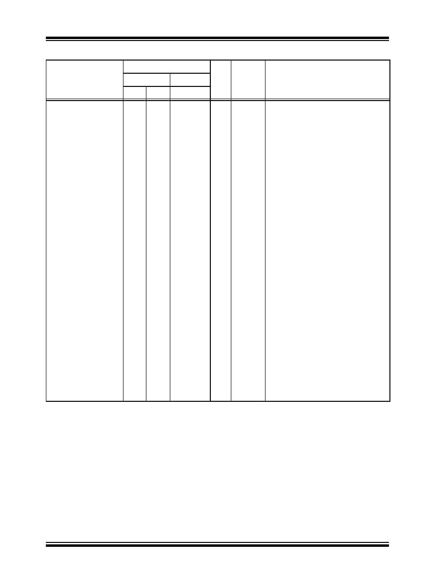
PORTB is a bidirectional I/O port. PORTB
can be software programmed for internal
weak pull-ups on all inputs.
RB0/INT0
RB0
INT0
48
60
58
I/O
I
TTL
ST
Digital I/O.
External interrupt 0.
RB1/INT1
RB1
INT1
47
59
57
I/O
I
TTL
ST
Digital I/O.
External interrupt 1.
RB2/INT2
RB2
INT2
46
58
56
I/O
I
TTL
ST
Digital I/O.
External interrupt 2.
RB3/INT3/CCP2
RB3
INT3
CCP2(1)
45
57
55
I/O
TTL
ST
Digital I/O.
External interrupt 3.
Capture 2 input/Compare 2 output/
PWM 2 output.
RB4/KBI0
RB4
KBI0
44
56
54
I/O
I
TTL
ST
Digital I/O.
Interrupt-on-change pin.
RB5/KBI1/PGM
RB5
KBI1
PGM
43
55
53
I/O
I
I/O
TTL
ST
Digital I/O.
Interrupt-on-change pin.
Low-Voltage ICSP Programming
enable pin.
RB6/KBI2/PGC
RB6
KBI2
PGC
42
54
52
I/O
I
I/O
TTL
ST
Digital I/O.
Interrupt-on-change pin.
In-circuit debugger and ICSP
programming clock.
RB7/KBI3/PGD
RB7
KBI3
PGD
37
48
47
I/O
TTL
ST
Digital I/O.
Interrupt-on-change pin.
In-circuit debugger and ICSP
programming data.
TABLE 1-2:
PIC18F6585/8585/6680/8680 PINOUT I/O DESCRIPTIONS (CONTINUED)
Pin Name
Pin Number
Pin
Type
Buffer
Type
Description
PIC18F6X8X PIC18F8X8X
TQFP PLCC
TQFP
Legend: TTL
= TTL compatible input
CMOS
= CMOS compatible input or output
ST
= Schmitt Trigger input with CMOS levels
Analog = Analog input
I
= Input
O
= Output
P
= Power
OD
= Open-Drain (no P diode to VDD)
Note 1:
Alternate assignment for CCP2 in all operating modes except Microcontroller – applies to PIC18F8X8X only.
2:
Default assignment when CCP2MX is set.
3:
External memory interface functions are only available on PIC18F8X8X devices.
4:
CCP2 is multiplexed with this pin by default when configured in Microcontroller mode; otherwise, it is
multiplexed with either RB3 or RC1.
5:
PORTH and PORTJ are only available on PIC18F8X8X (80-pin) devices.
6:
PSP is available in Microcontroller mode only.
7:
On PIC18F8X8X devices, these pins can be multiplexed with RH7/RH6 by changing the ECCPMX
configuration bit.
相关PDF资料 |
PDF描述 |
|---|---|
| 0982660125 | CBL 12POS 0.5MM JMPR TYPE A 5" |
| GBM25DCTT | CONN EDGECARD 50POS DIP .156 SLD |
| ESC05DTEH | CONN EDGECARD 10POS .100 EYELET |
| GCM22DCCN | CONN EDGECARD 44POS R/A .156 SLD |
| PCM16YN0 | MODULE PROC FOR PIC16F785 |
相关代理商/技术参数 |
参数描述 |
|---|---|
| PCM18XL0 | 功能描述:插座和适配器 Processor MOD RoHS:否 制造商:Silicon Labs 产品:Adapter 用于:EM35x |
| PCM18XM0 | 制造商:Microchip Technology Inc 功能描述:PROCESSOR MODULE |
| PCM18XN0 | 功能描述:插座和适配器 - RoHS:否 制造商:Silicon Labs 产品:Adapter 用于:EM35x |
| PCM18XN1 | 功能描述:插座和适配器 PIC18F4525 Proc Mod RoHS:否 制造商:Silicon Labs 产品:Adapter 用于:EM35x |
| PCM18XP0 | 功能描述:插座和适配器 - RoHS:否 制造商:Silicon Labs 产品:Adapter 用于:EM35x |
发布紧急采购,3分钟左右您将得到回复。