- 您现在的位置:买卖IC网 > PDF目录17011 > PCM18XK1 (Microchip Technology)MODULE PROC PIC18F8680,6680,8565 PDF资料下载
参数资料
| 型号: | PCM18XK1 |
| 厂商: | Microchip Technology |
| 文件页数: | 75/424页 |
| 文件大小: | 0K |
| 描述: | MODULE PROC PIC18F8680,6680,8565 |
| 标准包装: | 1 |
| 附件类型: | 处理器模块 |
| 适用于相关产品: | ICE2000 |
| 产品目录页面: | 658 (CN2011-ZH PDF) |
| 配用: | ICE2000-ND - EMULATOR MPLAB-ICE 2000 POD |
| 相关产品: | DVA18PQ802-ND - DEVICE ATP FOR ICE2000 |
第1页第2页第3页第4页第5页第6页第7页第8页第9页第10页第11页第12页第13页第14页第15页第16页第17页第18页第19页第20页第21页第22页第23页第24页第25页第26页第27页第28页第29页第30页第31页第32页第33页第34页第35页第36页第37页第38页第39页第40页第41页第42页第43页第44页第45页第46页第47页第48页第49页第50页第51页第52页第53页第54页第55页第56页第57页第58页第59页第60页第61页第62页第63页第64页第65页第66页第67页第68页第69页第70页第71页第72页第73页第74页当前第75页第76页第77页第78页第79页第80页第81页第82页第83页第84页第85页第86页第87页第88页第89页第90页第91页第92页第93页第94页第95页第96页第97页第98页第99页第100页第101页第102页第103页第104页第105页第106页第107页第108页第109页第110页第111页第112页第113页第114页第115页第116页第117页第118页第119页第120页第121页第122页第123页第124页第125页第126页第127页第128页第129页第130页第131页第132页第133页第134页第135页第136页第137页第138页第139页第140页第141页第142页第143页第144页第145页第146页第147页第148页第149页第150页第151页第152页第153页第154页第155页第156页第157页第158页第159页第160页第161页第162页第163页第164页第165页第166页第167页第168页第169页第170页第171页第172页第173页第174页第175页第176页第177页第178页第179页第180页第181页第182页第183页第184页第185页第186页第187页第188页第189页第190页第191页第192页第193页第194页第195页第196页第197页第198页第199页第200页第201页第202页第203页第204页第205页第206页第207页第208页第209页第210页第211页第212页第213页第214页第215页第216页第217页第218页第219页第220页第221页第222页第223页第224页第225页第226页第227页第228页第229页第230页第231页第232页第233页第234页第235页第236页第237页第238页第239页第240页第241页第242页第243页第244页第245页第246页第247页第248页第249页第250页第251页第252页第253页第254页第255页第256页第257页第258页第259页第260页第261页第262页第263页第264页第265页第266页第267页第268页第269页第270页第271页第272页第273页第274页第275页第276页第277页第278页第279页第280页第281页第282页第283页第284页第285页第286页第287页第288页第289页第290页第291页第292页第293页第294页第295页第296页第297页第298页第299页第300页第301页第302页第303页第304页第305页第306页第307页第308页第309页第310页第311页第312页第313页第314页第315页第316页第317页第318页第319页第320页第321页第322页第323页第324页第325页第326页第327页第328页第329页第330页第331页第332页第333页第334页第335页第336页第337页第338页第339页第340页第341页第342页第343页第344页第345页第346页第347页第348页第349页第350页第351页第352页第353页第354页第355页第356页第357页第358页第359页第360页第361页第362页第363页第364页第365页第366页第367页第368页第369页第370页第371页第372页第373页第374页第375页第376页第377页第378页第379页第380页第381页第382页第383页第384页第385页第386页第387页第388页第389页第390页第391页第392页第393页第394页第395页第396页第397页第398页第399页第400页第401页第402页第403页第404页第405页第406页第407页第408页第409页第410页第411页第412页第413页第414页第415页第416页第417页第418页第419页第420页第421页第422页第423页第424页
PIC18F6585/8585/6680/8680
DS30491C-page 164
2004 Microchip Technology Inc.
14.0
TIMER3 MODULE
The Timer3 module timer/counter has the following
features:
16-bit timer/counter
(two 8-bit registers; TMR3H and TMR3L)
Readable and writable (both registers)
Internal or external clock select
Interrupt on overflow from FFFFh to 0000h
Reset from CCP module trigger
Figure 14-1 is a simplified block diagram of the Timer3
module.
Register 14-1 shows the Timer3 Control register. This
register controls the operating mode of the Timer3
module and sets the Enhanced CCP1 and CCP2 clock
source.
Register 12-1 shows the Timer1 Control register. This
register controls the operating mode of the Timer1
module, as well as containing the Timer1 oscillator
enable bit (T1OSCEN) which can be a clock source for
Timer3.
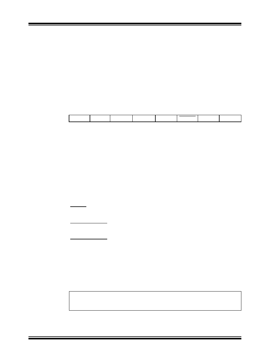
REGISTER 14-1:
T3CON: TIMER3 CONTROL REGISTER
R/W-0
RD16
T3CCP2
T3CKPS1
T3CKPS0
T3CCP1
T3SYNC
TMR3CS
TMR3ON
bit 7
bit 0
bit 7
RD16: 16-bit Read/Write Mode Enable bit
1
= Enables register read/write of Timer3 in one 16-bit operation
0
= Enables register read/write of Timer3 in two 8-bit operations
bit 6, 3
T3CCP2:T3CCP1: Timer3 and Timer1 to CCPx Enable bits
1x
= Timer3 is the clock source for compare/capture of CCP1 and CCP2 modules
01
= Timer3 is the clock source for compare/capture of CCP2 module,
Timer1 is the clock source for compare/capture of CCP1 module
00
= Timer1 is the clock source for compare/capture of CCP1 and CCP2 modules
bit 5-4
T3CKPS1:T3CKPS0: Timer3 Input Clock Prescale Select bits
11
= 1:8 prescale value
10
= 1:4 prescale value
01
= 1:2 prescale value
00
= 1:1 prescale value
bit 2
T3SYNC: Timer3 External Clock Input Synchronization Control bit
(Not usable if the system clock comes from Timer1/Timer3.)
When TMR3CS = 1:
1
= Do not synchronize external clock input
0
= Synchronize external clock input
When TMR3CS = 0:
This bit is ignored. Timer3 uses the internal clock when TMR3CS = 0.
bit 1
TMR3CS: Timer3 Clock Source Select bit
1
= External clock input from Timer1 oscillator or T13CKI
(on the rising edge after the first falling edge)
0
= Internal clock (FOSC/4)
bit 0
TMR3ON: Timer3 On bit
1
= Enables Timer3
0
= Stops Timer3
Legend:
R = Readable bit
W = Writable bit
U = Unimplemented bit, read as ‘0’
- n = Value at POR
‘1’ = Bit is set
‘0’ = Bit is cleared
x = Bit is unknown
相关PDF资料 |
PDF描述 |
|---|---|
| 0982660125 | CBL 12POS 0.5MM JMPR TYPE A 5" |
| GBM25DCTT | CONN EDGECARD 50POS DIP .156 SLD |
| ESC05DTEH | CONN EDGECARD 10POS .100 EYELET |
| GCM22DCCN | CONN EDGECARD 44POS R/A .156 SLD |
| PCM16YN0 | MODULE PROC FOR PIC16F785 |
相关代理商/技术参数 |
参数描述 |
|---|---|
| PCM18XL0 | 功能描述:插座和适配器 Processor MOD RoHS:否 制造商:Silicon Labs 产品:Adapter 用于:EM35x |
| PCM18XM0 | 制造商:Microchip Technology Inc 功能描述:PROCESSOR MODULE |
| PCM18XN0 | 功能描述:插座和适配器 - RoHS:否 制造商:Silicon Labs 产品:Adapter 用于:EM35x |
| PCM18XN1 | 功能描述:插座和适配器 PIC18F4525 Proc Mod RoHS:否 制造商:Silicon Labs 产品:Adapter 用于:EM35x |
| PCM18XP0 | 功能描述:插座和适配器 - RoHS:否 制造商:Silicon Labs 产品:Adapter 用于:EM35x |
发布紧急采购,3分钟左右您将得到回复。