- 您现在的位置:买卖IC网 > PDF目录271228 > S71PL254JC0BAITU3 (SPANSION LLC) SPECIALTY MEMORY CIRCUIT, PBGA84 PDF资料下载
参数资料
| 型号: | S71PL254JC0BAITU3 |
| 厂商: | SPANSION LLC |
| 元件分类: | 存储器 |
| 英文描述: | SPECIALTY MEMORY CIRCUIT, PBGA84 |
| 封装: | 8 X 11.60 MM, 1.40 MM HEIGHT, FBGA-84 |
| 文件页数: | 113/188页 |
| 文件大小: | 5078K |
| 代理商: | S71PL254JC0BAITU3 |
第1页第2页第3页第4页第5页第6页第7页第8页第9页第10页第11页第12页第13页第14页第15页第16页第17页第18页第19页第20页第21页第22页第23页第24页第25页第26页第27页第28页第29页第30页第31页第32页第33页第34页第35页第36页第37页第38页第39页第40页第41页第42页第43页第44页第45页第46页第47页第48页第49页第50页第51页第52页第53页第54页第55页第56页第57页第58页第59页第60页第61页第62页第63页第64页第65页第66页第67页第68页第69页第70页第71页第72页第73页第74页第75页第76页第77页第78页第79页第80页第81页第82页第83页第84页第85页第86页第87页第88页第89页第90页第91页第92页第93页第94页第95页第96页第97页第98页第99页第100页第101页第102页第103页第104页第105页第106页第107页第108页第109页第110页第111页第112页当前第113页第114页第115页第116页第117页第118页第119页第120页第121页第122页第123页第124页第125页第126页第127页第128页第129页第130页第131页第132页第133页第134页第135页第136页第137页第138页第139页第140页第141页第142页第143页第144页第145页第146页第147页第148页第149页第150页第151页第152页第153页第154页第155页第156页第157页第158页第159页第160页第161页第162页第163页第164页第165页第166页第167页第168页第169页第170页第171页第172页第173页第174页第175页第176页第177页第178页第179页第180页第181页第182页第183页第184页第185页第186页第187页第188页
May 21, 2004 S29PL127_064_032J_00_A1
S29PL127J/S29PL064J/S29PL032J for MCP
29
Prelimin ary
Device Bus Operations
This section describes the requirements and use of the device bus operations,
which are initiated through the internal command register. The command register
itself does not occupy any addressable memory location. The register is a latch
used to store the commands, along with the address and data information
needed to execute the command. The contents of the register serve as inputs to
the internal state machine. The state machine outputs dictate the function of the
device. Table 1 lists the device bus operations, the inputs and control levels they
require, and the resulting output. The following subsections describe each of
these operations in further detail.
Legend: L= Logic Low = VIL, H = Logic High = VIH, VID = 11.5-12.5 V, VHH = 8.5-9.5 V, X = Don’t Care, SA =
Sector Address, AIN = Address In, DIN = Data In, DOUT = Data Out
Notes:
1. The sector protect and sector unprotect functions may also be implemented via programming equipment. See the
High Voltage Sector Protection section.
2. WP#/ACC must be high when writing to upper two and lower two sectors.
Requirements for Reading Array Data
To read array data from the outputs, the system must drive the OE# and appro-
priate CE# pins. OE# is the output control and gates array data to the output
pins. WE# should remain at VIH.
The internal state machine is set for reading array data upon device power-up,
or after a hardware reset. This ensures that no spurious alteration of the memory
content occurs during the power transition. No command is necessary in this
mode to obtain array data. Standard microprocessor read cycles that assert valid
addresses on the device address inputs produce valid data on the device data
outputs. Each bank remains enabled for read access until the command register
contents are altered.
ICC1 in the DC Characteristics table represents the active current specification for
reading array data.
Random Read (Non-Page Read)
Address access time (tACC) is equal to the delay from stable addresses to valid
output data. The chip enable access time (tCE) is the delay from the stable ad-
dresses and stable CE# to valid data at the output inputs. The output enable
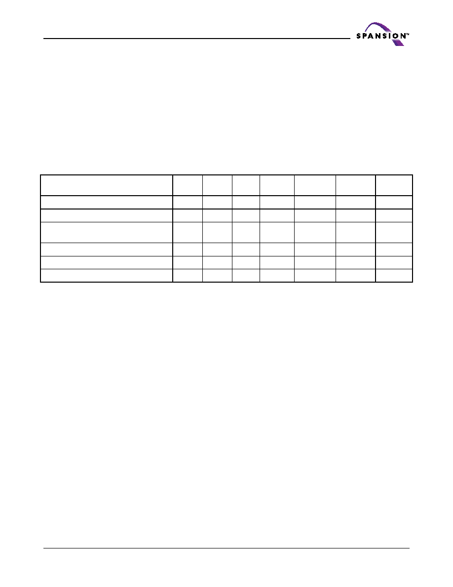
Table 1. PL127J Device Bus Operations
Operation
CE#
OE#
WE#
RESET#
WP#/ACC
Addresses
(Amax–A0)
DQ15–
DQ0
Read
L
H
X
AIN
DOUT
Write
L
H
L
H
X (Note 2)
AIN
DIN
Standby
VIO±
0.3 V
X
VIO ±
0.3 V
X (Note 2)
X
High-Z
Output Disable
L
H
X
High-Z
Reset
X
L
X
High-Z
Temporary Sector Unprotect (High Voltage)
X
VID
X
AIN
DIN
相关PDF资料 |
PDF描述 |
|---|---|
| S71PL032JF0BFW074 | SPECIALTY MEMORY CIRCUIT, PBGA56 |
| S29AL016D90MFN011 | 1M X 16 FLASH 3V PROM, 90 ns, PDSO44 |
| SM-5MIN-A-TL-26 | RF COAXIAL RELAY, SP5T, FAILSAFE, 2875mW (COIL), 26500MHz, PANEL MOUNT |
| SM-5MIN-A-TL | RF COAXIAL RELAY, SP5T, FAILSAFE, 2875mW (COIL), 18000MHz, PANEL MOUNT |
| SM-5MIN-A | RF COAXIAL RELAY, SP5T, FAILSAFE, 2875mW (COIL), 18000MHz, PANEL MOUNT |
相关代理商/技术参数 |
参数描述 |
|---|---|
| S71PL254JC0BAW0Z0 | 制造商:SPANSION 制造商全称:SPANSION 功能描述:Based MCPs |
| S71PL254JC0BAW0Z2 | 制造商:SPANSION 制造商全称:SPANSION 功能描述:Based MCPs |
| S71PL254JC0BAW0Z3 | 制造商:SPANSION 制造商全称:SPANSION 功能描述:Based MCPs |
| S71PL254JC0BAW9Z0 | 制造商:SPANSION 制造商全称:SPANSION 功能描述:Based MCPs |
| S71PL254JC0BAW9Z2 | 制造商:SPANSION 制造商全称:SPANSION 功能描述:Based MCPs |
发布紧急采购,3分钟左右您将得到回复。