- 您现在的位置:买卖IC网 > PDF目录136930 > TLC320AC01CPMR (TEXAS INSTRUMENTS INC) SPECIALTY ANALOG CIRCUIT, PQFP64 PDF资料下载
参数资料
| 型号: | TLC320AC01CPMR |
| 厂商: | TEXAS INSTRUMENTS INC |
| 元件分类: | 模拟信号调理 |
| 英文描述: | SPECIALTY ANALOG CIRCUIT, PQFP64 |
| 封装: | PLASTIC, QFP-64 |
| 文件页数: | 9/93页 |
| 文件大小: | 601K |
| 代理商: | TLC320AC01CPMR |
第1页第2页第3页第4页第5页第6页第7页第8页当前第9页第10页第11页第12页第13页第14页第15页第16页第17页第18页第19页第20页第21页第22页第23页第24页第25页第26页第27页第28页第29页第30页第31页第32页第33页第34页第35页第36页第37页第38页第39页第40页第41页第42页第43页第44页第45页第46页第47页第48页第49页第50页第51页第52页第53页第54页第55页第56页第57页第58页第59页第60页第61页第62页第63页第64页第65页第66页第67页第68页第69页第70页第71页第72页第73页第74页第75页第76页第77页第78页第79页第80页第81页第82页第83页第84页第85页第86页第87页第88页第89页第90页第91页第92页第93页
2–4
2.3
Master-Slave Terminal Function
Table 2–1 describes the function of the master/slave (M/S) input. The only difference between master and
slave operations in the TLC320AC01 is that SCLK and FS are outputs when M/S is high and inputs when
M/S is low.
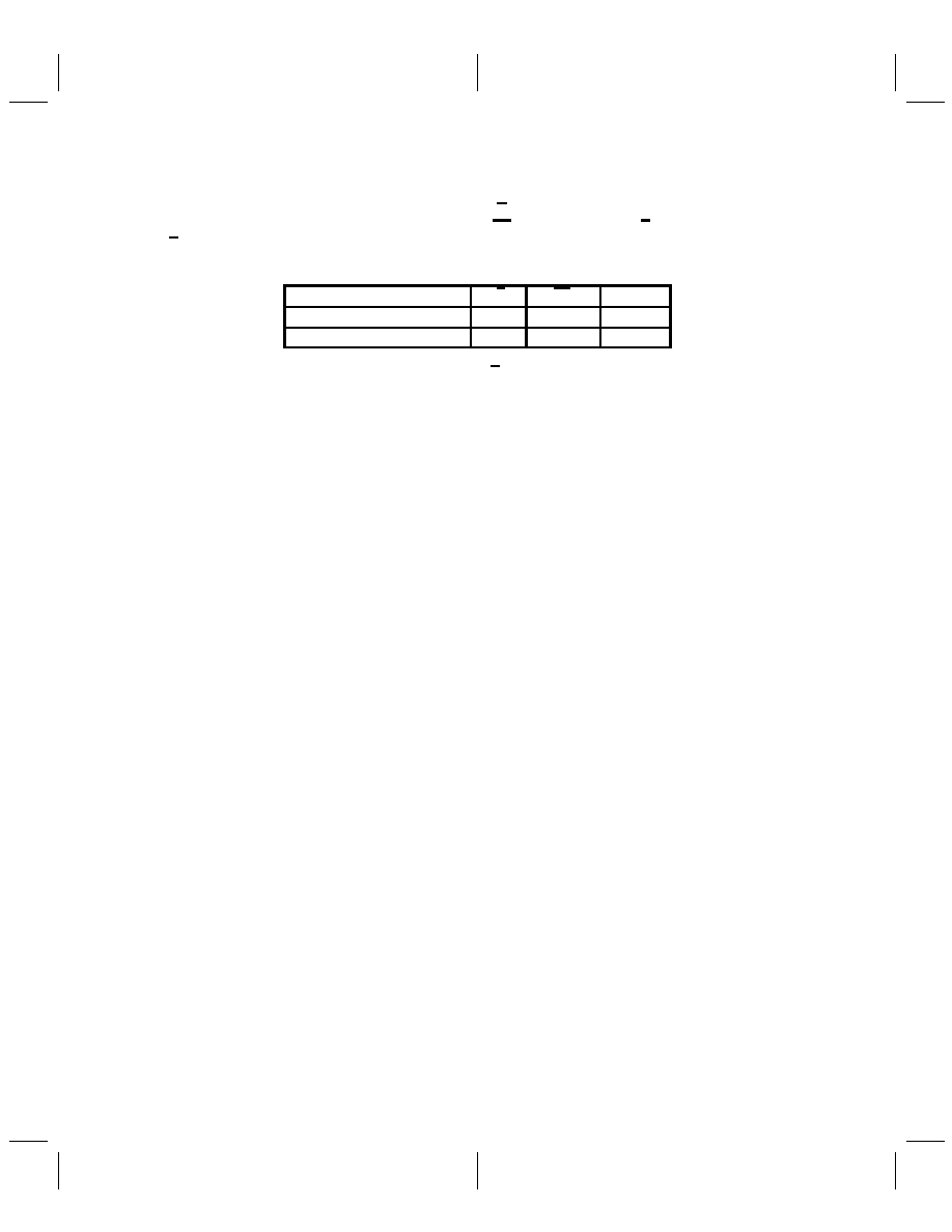
Table 2–1. Master-Slave Selection
MODE
M/S
FS
SCLK
Master and Stand Alone
H
Output
Slave and Codec Emulation
L
Input
When the stand-alone mode is desired or when the device is
permanently in the master mode, M/S must be high.
2.4
ADC Signal Channel
To produce excellent common-mode rejection of unwanted signals, the analog signal is processed
differentially until it is converted to digital data. The signal is amplified by the input amplifier at one of three
software-selectable gains (typically 0 dB, 6 dB, or 12 dB). A squelch mode can also be programmed for the
input amplifier.
The amplifier output is filtered and applied to the ADC input. The ADC converts the signal into discrete digital
words in 2s-complement format corresponding to the analog-signal value at the sampling time. These 16-bit
digital words, representing sampled values of the analog input signal, are clocked out of the serial port
(DOUT), one word for each primary communication interval. During secondary communications, the data
previously programmed into the registers can be read out with the appropriate register address and with the
read bit set to 1. When a register read is not requested, all 16 bits are 0.
2.5
DAC Signal Channel
DIN receives the 16-bit serial data word (2s complement) from the host during the primary communications
interval and latches the data on the seventeenth rising edge of SCLK. The data are converted to an analog
voltage by the DAC with a sample and hold and then through a (sin x)/x correction circuit and a smoothing
filter. An output buffer with three software-programmable gains (0 dB, – 6 dB, and – 12 dB), as shown in
register 4, drives the differential outputs OUT + and OUT –. A squelch mode can also be programmed for
the output buffer. During secondary communications, the configuration program data are read into the
device control registers.
2.6
Serial Interface
The digital serial interface consists of the shift clock, the frame-synchronization signal, the ADC-channel
data output, and the DAC-channel data input. During the primary 16-bit frame-synchronization interval, the
SCLK transfers the ADC channel results from DOUT and transfers 16-bit DAC data into DIN.
During the secondary frame-synchronization interval, the SCLK transfers the register read data from DOUT
when the read bit is set to a 1. In addition, the SCLK transfers control and device parameter information into
DIN. The functional sequence is shown in Figure 2–1.
相关PDF资料 |
PDF描述 |
|---|---|
| TC6501P095VCTTR | SPECIALTY ANALOG CIRCUIT, PDSO5 |
| TS5A63157YZPR | 1-CHANNEL, SGL POLE DOUBLE THROW SWITCH, BGA6 |
| TLC2933AIPW | PHASE LOCKED LOOP, 32 MHz, PDSO14 |
| TPS2560DRC | 1-CHANNEL POWER SUPPLY SUPPORT CKT, PDSO10 |
| TS4040DIZ-2.5 | 1-OUTPUT TWO TERM VOLTAGE REFERENCE, 2.5 V, PBCY3 |
相关代理商/技术参数 |
参数描述 |
|---|---|
| TLC320AC02 | 制造商:TI 制造商全称:Texas Instruments 功能描述:Single-Supply Analog Interface Circuit |
| TLC320AC02C | 制造商:TI 制造商全称:Texas Instruments 功能描述:Single-Supply Analog Interface Circuit |
| TLC320AC02CFN | 功能描述:接口—CODEC SNGL CH Codec Bandwidth Indpendent RoHS:否 制造商:Texas Instruments 类型: 分辨率: 转换速率:48 kSPs 接口类型:I2C ADC 数量:2 DAC 数量:4 工作电源电压:1.8 V, 2.1 V, 2.3 V to 5.5 V 最大工作温度:+ 85 C 安装风格:SMD/SMT 封装 / 箱体:DSBGA-81 封装:Reel |
| TLC320AC02CFNR | 功能描述:接口—CODEC SNGL CH Codec Bandwidth Indpendent RoHS:否 制造商:Texas Instruments 类型: 分辨率: 转换速率:48 kSPs 接口类型:I2C ADC 数量:2 DAC 数量:4 工作电源电压:1.8 V, 2.1 V, 2.3 V to 5.5 V 最大工作温度:+ 85 C 安装风格:SMD/SMT 封装 / 箱体:DSBGA-81 封装:Reel |
| TLC320AC02CPM | 功能描述:接口—CODEC SNGL CH Codec Bandwidth Indpendent RoHS:否 制造商:Texas Instruments 类型: 分辨率: 转换速率:48 kSPs 接口类型:I2C ADC 数量:2 DAC 数量:4 工作电源电压:1.8 V, 2.1 V, 2.3 V to 5.5 V 最大工作温度:+ 85 C 安装风格:SMD/SMT 封装 / 箱体:DSBGA-81 封装:Reel |
发布紧急采购,3分钟左右您将得到回复。