- 您现在的位置:买卖IC网 > PDF目录68427 > W25Q16DWZPIP (WINBOND ELECTRONICS CORP) 16M X 1 SPI BUS SERIAL EEPROM, PDSO8 PDF资料下载
参数资料
| 型号: | W25Q16DWZPIP |
| 厂商: | WINBOND ELECTRONICS CORP |
| 元件分类: | PROM |
| 英文描述: | 16M X 1 SPI BUS SERIAL EEPROM, PDSO8 |
| 封装: | 6 X 5 MM, GREEN , PLASTIC, WSON-8 |
| 文件页数: | 59/83页 |
| 文件大小: | 1268K |
| 代理商: | W25Q16DWZPIP |
第1页第2页第3页第4页第5页第6页第7页第8页第9页第10页第11页第12页第13页第14页第15页第16页第17页第18页第19页第20页第21页第22页第23页第24页第25页第26页第27页第28页第29页第30页第31页第32页第33页第34页第35页第36页第37页第38页第39页第40页第41页第42页第43页第44页第45页第46页第47页第48页第49页第50页第51页第52页第53页第54页第55页第56页第57页第58页当前第59页第60页第61页第62页第63页第64页第65页第66页第67页第68页第69页第70页第71页第72页第73页第74页第75页第76页第77页第78页第79页第80页第81页第82页第83页
W25Q16DW
- 62 -
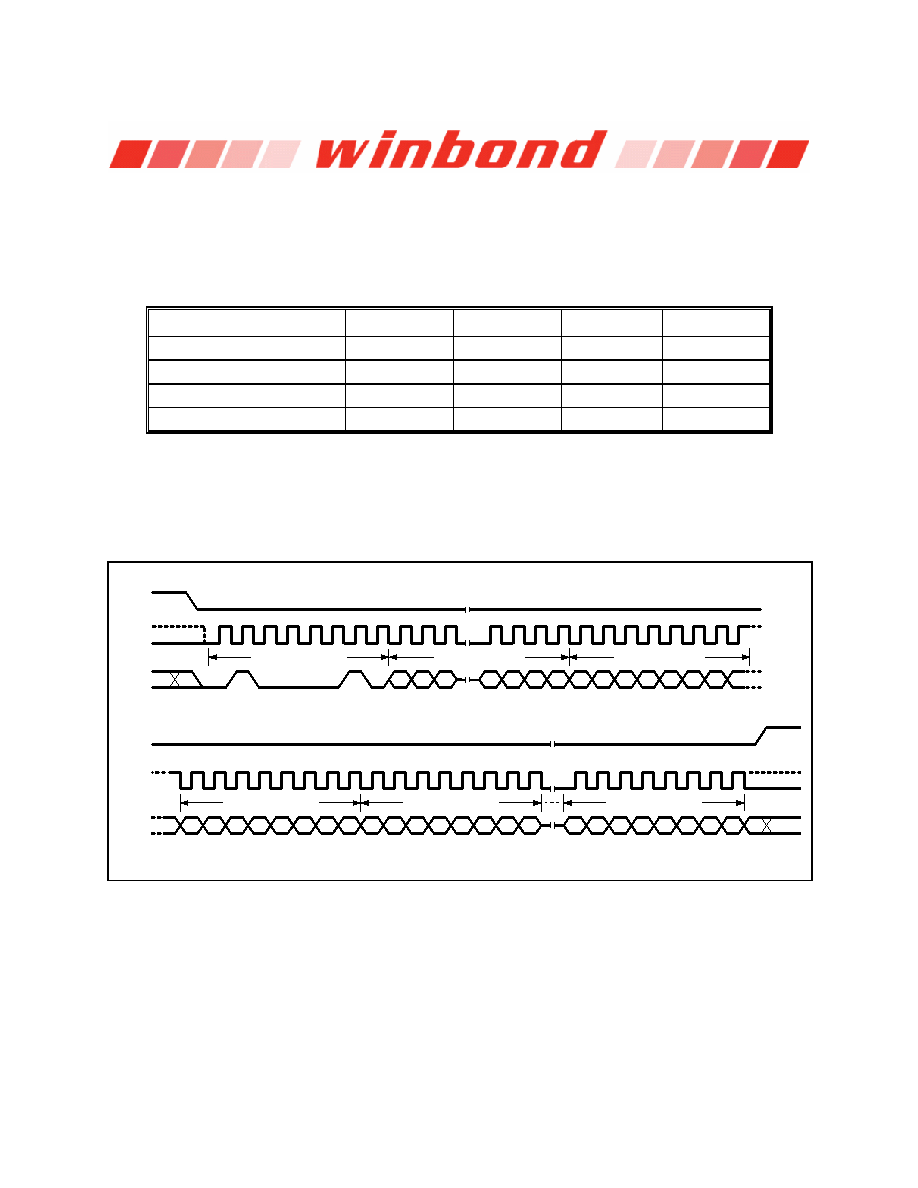
10.2.36 Program Security Registers (42h)
The Program Security Register instruction is similar to the Page Program instruction. It allows from one
byte to 256 bytes of security register data to be programmed at previously erased (FFh) memory locations.
A Write Enable instruction must be executed before the device will accept the Program Security Register
Instruction (Status Register bit WEL= 1). The instruction is initiated by driving the /CS pin low then shifting
the instruction code “42h” followed by a 24-bit address (A23-A0) and at least one data byte, into the DI pin.
The /CS pin must be held low for the entire length of the instruction while data is being sent to the device.
ADDRESS
A23-16
A15-12
A11-8
A7-0
Security Register #0*
00h
0 0 0 0
Byte Address
Security Register #1
00h
0 0 0 1
0 0 0 0
Byte Address
Security Register #2
00h
0 0 1 0
0 0 0 0
Byte Address
Security Register #3
00h
0 0 1 1
0 0 0 0
Byte Address
*
Please note that Security Register 0 is Reserved by Winbond for future use. It is
recommended to use Security registers 1- 3 before using register 0.
The Program Security Register instruction sequence is shown in Figure 35. The Security Register Lock
Bits (LB3-0) in the Status Register-2 can be used to OTP protect the security registers. Once a lock bit is
set to 1, the corresponding security register will be permanently locked, Program Security Register
instruction to that register will be ignored (See 11.1.9, 11.2.21 for detail descriptions).
/CS
CLK
DI
(IO
0)
Mode 0
Mode 3
0
1
2
3
4
5
6
7
Instruction (42h)
8
9
10
28
29
30
39
24-Bit Address
23
22
21
3
2
1
*
/CS
CLK
40
DI
(IO
0)
41
42
43
44
45
46
47
Data Byte 2
48
49
50
52
53
54
55
20
72
7
6
5
4
3
2
1
0
51
39
0
31
0
32
33
34
35
36
37
38
Data Byte 1
7
6
5
4
3
2
1
*
Mode 0
Mode 3
Data Byte 3
20
73
20
74
20
75
20
76
20
77
20
78
20
79
0
Data Byte 256
*
7
6
5
4
3
2
1
0
*
7
6
5
4
3
2
1
0
*
= MSB
*
Figure 35. Program Security Registers Instruction (SPI Mode only)
相关PDF资料 |
PDF描述 |
|---|---|
| W25Q20BWUXIP | 2M X 1 SPI BUS SERIAL EEPROM, PDSO8 |
| W25Q32BVSSAG | 32M X 1 SPI BUS SERIAL EEPROM, PDSO8 |
| W25Q32BVSSAP | 32M X 1 SPI BUS SERIAL EEPROM, PDSO8 |
| W25Q32BWSNIP | 4M X 8 SPI BUS SERIAL EEPROM, DSO8 |
| W25Q32BWSSIG | 4M X 8 SPI BUS SERIAL EEPROM, PDSO8 |
相关代理商/技术参数 |
参数描述 |
|---|---|
| W25Q16V | 制造商:WINBOND 制造商全称:Winbond 功能描述:16M-BIT SERIAL FLASH MEMORY WITH DUAL AND QUAD SPI |
| W25Q16VSFIG | 功能描述:IC FLASH 16MBIT 80MHZ 16SOIC RoHS:是 类别:集成电路 (IC) >> 存储器 系列:SpiFlash® 产品变化通告:Product Discontinuation 26/Apr/2010 标准包装:136 系列:- 格式 - 存储器:RAM 存储器类型:SRAM - 同步,DDR II 存储容量:18M(1M x 18) 速度:200MHz 接口:并联 电源电压:1.7 V ~ 1.9 V 工作温度:0°C ~ 70°C 封装/外壳:165-TBGA 供应商设备封装:165-CABGA(13x15) 包装:托盘 其它名称:71P71804S200BQ |
| W25Q16VSSIG | 功能描述:IC FLASH 16MBIT 80MHZ 8SOIC RoHS:是 类别:集成电路 (IC) >> 存储器 系列:SpiFlash® 产品变化通告:Product Discontinuation 26/Apr/2010 标准包装:136 系列:- 格式 - 存储器:RAM 存储器类型:SRAM - 同步,DDR II 存储容量:18M(1M x 18) 速度:200MHz 接口:并联 电源电压:1.7 V ~ 1.9 V 工作温度:0°C ~ 70°C 封装/外壳:165-TBGA 供应商设备封装:165-CABGA(13x15) 包装:托盘 其它名称:71P71804S200BQ |
| W25Q16VZPIG | 制造商:WINBOND 制造商全称:Winbond 功能描述:16M-BIT SERIAL FLASH MEMORY WITH DUAL AND QUAD SPI |
| W25Q20BW | 制造商:WINBOND 制造商全称:Winbond 功能描述:1.8V 2M-BIT SERIAL FLASH MEMORY WITH DUAL AND QUAD SPI |
发布紧急采购,3分钟左右您将得到回复。