参数资料
| 型号: | XCF128XFTG64C |
| 厂商: | Xilinx Inc |
| 文件页数: | 64/88页 |
| 文件大小: | 0K |
| 描述: | IC PROM SRL 128M GATE 64-FTBGA |
| 标准包装: | 1 |
| 可编程类型: | 系统内可编程 |
| 存储容量: | 128Mb |
| 电源电压: | 1.7 V ~ 2 V |
| 工作温度: | -40°C ~ 85°C |
| 封装/外壳: | 64-TBGA |
| 供应商设备封装: | 64-TFBGA |
| 包装: | 托盘 |
| 产品目录页面: | 601 (CN2011-ZH PDF) |
| 其它名称: | 122-1578 |
第1页第2页第3页第4页第5页第6页第7页第8页第9页第10页第11页第12页第13页第14页第15页第16页第17页第18页第19页第20页第21页第22页第23页第24页第25页第26页第27页第28页第29页第30页第31页第32页第33页第34页第35页第36页第37页第38页第39页第40页第41页第42页第43页第44页第45页第46页第47页第48页第49页第50页第51页第52页第53页第54页第55页第56页第57页第58页第59页第60页第61页第62页第63页当前第64页第65页第66页第67页第68页第69页第70页第71页第72页第73页第74页第75页第76页第77页第78页第79页第80页第81页第82页第83页第84页第85页第86页第87页第88页
Platform Flash XL High-Density Configuration and Storage Device
DS617 (v3.0.1) January 07, 2010
Product Specification
67
R
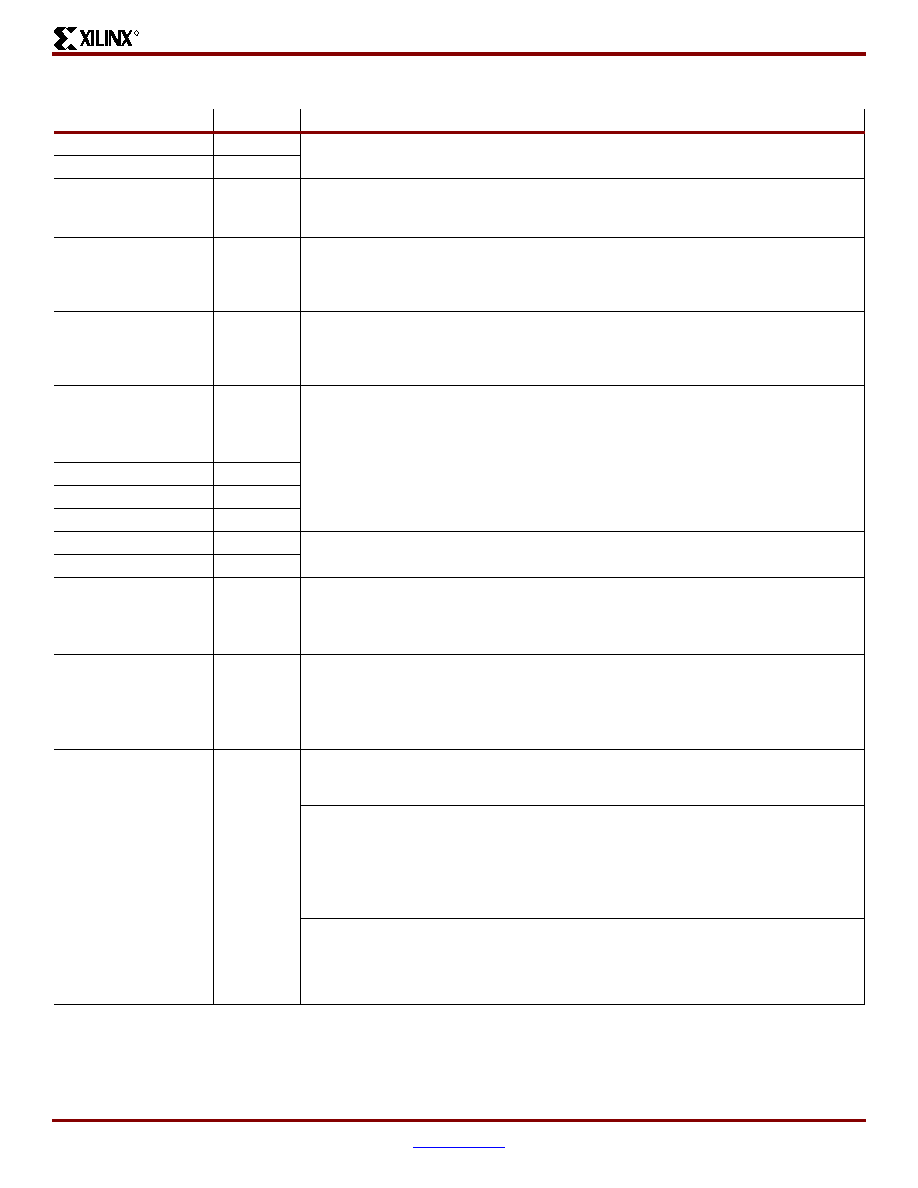
Table 44: Bank and Erase Block Region 1 Information(1,2)
Offset
Data
Description
(P+24)h = 12Eh
0Fh
Number of identical banks within Bank Region 1
(P+25)h = 12Fh
00h
(P+26)h = 130h
11h
Number of program or erase operations allowed in Bank Region 1:
Bits 0–3: Number of simultaneous program operations Bits
4–7: Number of simultaneous erase operations
(P+27)h = 131h
00h
Number of program or erase operations allowed in other banks while a bank in same region is
programming
Bits 0–3: Number of simultaneous program operations
Bits 4–7: Number of simultaneous erase operations
(P+28)h = 132h
00h
Number of program or erase operations allowed in other banks while a bank in this region is
erasing
Bits 0–3: Number of simultaneous program operations Bits
4–7: Number of simultaneous erase operations
(P+29)h = 133h
01h
Types of erase block regions in Bank Region 1 n = number of erase block regions with
contiguous same-sized erase blocks. Symmetrically blocked banks have one blocking
region(2).
(P+2A)h = 134h
07h
Bank Region 1 Erase Block Type 1 Information:
Bits 0–15: n+1 = number of identical-sized erase blocks
Bits 16–31: n×256 = number of bytes in erase block region
(P+2B)h = 135h
00h
(P+2C)h = 136h
00h
(P+2D)h = 137h
02h
(P+2E)h = 138h
64h
Bank Region 1 (Erase Block Type 1)
Minimum block erase cycles × 1000
(P+2F)h = 139h
00h
(P+30)h = 13Ah
01h
Bank Region 1 (Erase Block Type 1): BIts per cell, internal ECC
Bits 0–3: bits per cell in erase region
Bit 4: reserved for “internal ECC used”
BIts 5–7: reserved
(P+31)h = 13Bh
03h
Bank Region 1 (Erase Block Type 1): Page mode and Synchronous mode capabilities
Bit 0: Page-mode reads permitted
Bit 1: Synchronous reads permitted
Bit 2: Synchronous writes permitted
Bits 3–7: reserved
––
Bank Region 1 Erase Block Type 2 Information
Bits 0–15: n+1 = number of identical-sized erase blocks
Bits 16–31: n×256 = number of bytes in erase block region
Bank Region 1 (Erase Block Type 2)
Minimum block erase cycles × 1000
Bank Regions 1 (Erase Block Type 2): Bits per cell, internal ECC
Bits 0–3: bits per cell in erase region
Bit 4: reserved for “internal ECC used”
Bits 5–7: reserved
Bank Region 1 (Erase Block Type 2): Page mode and Synchronous mode capabilities
Bit 0: Page-mode reads permitted
Bit 1: Synchronous reads permitted
Bit 2: Synchronous writes permitted
Bits 3–7: reserved
Notes:
1.
The variable P is a pointer which is defined at CFI offset 015h.
2.
Bank Regions. There are two Bank Regions, see Table 35, page 61.
相关PDF资料 |
PDF描述 |
|---|---|
| XCF32PFS48C | IC PROM SRL 1.8V 32M 48CSBGA |
| XCR3256XL-7CS280C | IC CPLD 256MCELL 3.3V HP 280CSP |
| XCS10-3VQG100C | IC FPGA 5V C-TEMP 100-VQFP |
| XCV600E-8HQ240C | IC FPGA 1.8V C-TEMP 240-HQFP |
| XCV812E-8FG900C | IC FPGA 1.8V C-TEMP 900-FBGA |
相关代理商/技术参数 |
参数描述 |
|---|---|
| XCF128XFTG64CES | 制造商:Xilinx 功能描述: |
| XCF12-L4Z1 | 制造商:SAIA - BURGESS ELECTRONICS INC. 功能描述:Catalogue / XCF12-L4Z1 |
| XCF12-S1 | 制造商:SAIA - BURGESS ELECTRONICS INC. 功能描述:Catalogue / XCF12-S1 |
| XCF13-S1 | 制造商:SAIA - BURGESS ELECTRONICS INC. 功能描述:Catalogue / XCF13-S1 |
| XCF16P | 制造商:XILINX 制造商全称:XILINX 功能描述:Platform Flash In-System Programmable Configuration PROMs |
发布紧急采购,3分钟左右您将得到回复。