参数资料
| 型号: | XCF128XFTG64C |
| 厂商: | Xilinx Inc |
| 文件页数: | 78/88页 |
| 文件大小: | 0K |
| 描述: | IC PROM SRL 128M GATE 64-FTBGA |
| 标准包装: | 1 |
| 可编程类型: | 系统内可编程 |
| 存储容量: | 128Mb |
| 电源电压: | 1.7 V ~ 2 V |
| 工作温度: | -40°C ~ 85°C |
| 封装/外壳: | 64-TBGA |
| 供应商设备封装: | 64-TFBGA |
| 包装: | 托盘 |
| 产品目录页面: | 601 (CN2011-ZH PDF) |
| 其它名称: | 122-1578 |
第1页第2页第3页第4页第5页第6页第7页第8页第9页第10页第11页第12页第13页第14页第15页第16页第17页第18页第19页第20页第21页第22页第23页第24页第25页第26页第27页第28页第29页第30页第31页第32页第33页第34页第35页第36页第37页第38页第39页第40页第41页第42页第43页第44页第45页第46页第47页第48页第49页第50页第51页第52页第53页第54页第55页第56页第57页第58页第59页第60页第61页第62页第63页第64页第65页第66页第67页第68页第69页第70页第71页第72页第73页第74页第75页第76页第77页当前第78页第79页第80页第81页第82页第83页第84页第85页第86页第87页第88页
Platform Flash XL High-Density Configuration and Storage Device
DS617 (v3.0.1) January 07, 2010
Product Specification
8
R
as close as possible to the package). The PCB track widths should
be sufficient to carry the required VPP program and erase currents.
FPGA Configuration Overview
Platform Flash XL enables the rich set of FPGA
configuration features without additional glue logic. The
device delivers the FPGA bitstream at power-on through a
16-bit data bus at data rates up to 800 Mb/s. The FPGA can
also be configured from one of many design/revision
bitstreams stored in the device. These revision bitstreams
are accessed through the FPGA's MultiBoot addressing
and fallback features available in specific system
configurations with Platform Flash XL. For detailed
descriptions of the FPGA configuration features and
configuration procedure, refer to the respective FPGA
configuration user guide.
At a high level, the general procedure for FPGA
configuration from Platform Flash XL is as follows:
1.
A system event, such as power-up, initiates the FPGA
configuration process. The FPGA drives its INIT_B pin
Low while it clears its configuration memory. The
Platform Flash XL drives its READY_WAIT pin Low
during its reset period.
2.
When ready, the FPGA and Platform Flash XL release
their respective INIT_B and READY_WAIT pins. An
external resistor pulls the connected
INIT_B-READY_WAIT signal from Low to High,
synchronizing the start of the FPGA configuration
process.
3.
At the start of the configuration process, the FPGA
samples its mode pins to determine its configuration
mode. For Master BPI-Up mode, the FPGA outputs an
address to read from the flash. For Slave SelectMAP
mode, onboard resistors set the initial flash read
address.
4.
The Platform Flash XL latches the initial address from
the FPGA or from onboard resistor settings into its
internal address counter and the Platform Flash XL
outputs the first 16-bit word.
5.
The bitstream is synchronously transferred from the
Platform Flash XL to the FPGA. During each
successive FPGA CCLK period, the Platform Flash XL
increments its internal address counter and outputs the
next 16-bit word of the bitstream for the FPGA to
consume.
6.
At the end of the configuration process, the FPGA starts
operation of the loaded bitstream and either drives
DONE High or releases DONE to High, indicating the
completion of the configuration procedure.
Platform Flash XL can configure the FPGA in Slave
SelectMAP (x16) (recommended for maximum
performance), Master SelectMAP (x16), or Master BPI-Up
(x16) configuration mode. See Table 4 for a summary of
attributes for different configuration modes and memories.
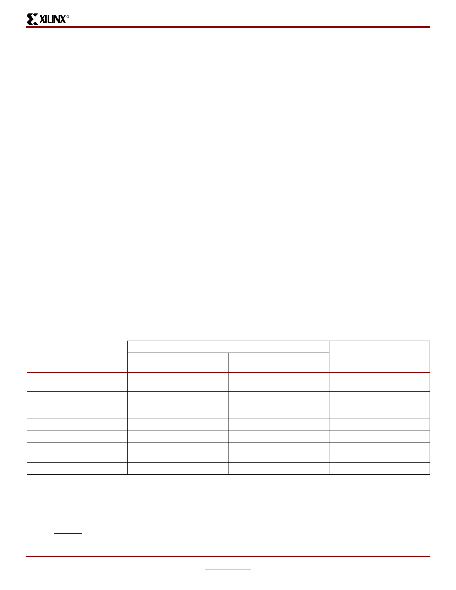
Table 4: Overview of FPGA Configuration from Platform Flash XL and Standard BPI Flash
Platform Flash XL
Third-Party Standard BPI
Flash
(110-ns Access Time)
High-Performance
Configuration Mode
Standard BPI Flash
Compatibility Mode
FPGA Configuration Mode
Slave SelectMAP mode
(x16 data bus width)
Master BPI-Up mode
(x16 data bus width)
Master BPI-Up mode
(x16 data bus width)
Guaranteed Bitstream
Transfer Bandwidth at Best
Clock Setting
800 Mb/s(1)
248 Mb/s(2)
78 Mb/s(3)
Virtex-5 FPGA Support
Virtex-6 FPGA Support
ISE Software Programming
Support
For limited setups(4)
MultiBoot Capable
Notes:
1.
The 800 Mb/s rate is achieved using a Virtex-5 FPGA with an external 50 MHz configuration clock source. Specific speed grades of the
Virtex-6 FPGA or system-level considerations can limit the configuration performance to less than 800 Mb/s.
2.
Bandwidth is based on an example Virtex-5 FPGA considering FMCCKTOL and BitGen ConfigRate = 31 MHz (nominal frequency).
3.
Bandwidth is based on an example Virtex-5 FPGA considering FMCCKTOL and BitGen ConfigRate = 17 MHz (nominal frequency),
bpi_page_size = 4, and bpi_1st_read_cycle = 4. First word access time = 110 ns; Page word access time = 25 ns.
4.
See XAPP973, Indirect Programming of BPI PROMs with Virtex-5 FPGAs.
相关PDF资料 |
PDF描述 |
|---|---|
| XCF32PFS48C | IC PROM SRL 1.8V 32M 48CSBGA |
| XCR3256XL-7CS280C | IC CPLD 256MCELL 3.3V HP 280CSP |
| XCS10-3VQG100C | IC FPGA 5V C-TEMP 100-VQFP |
| XCV600E-8HQ240C | IC FPGA 1.8V C-TEMP 240-HQFP |
| XCV812E-8FG900C | IC FPGA 1.8V C-TEMP 900-FBGA |
相关代理商/技术参数 |
参数描述 |
|---|---|
| XCF128XFTG64CES | 制造商:Xilinx 功能描述: |
| XCF12-L4Z1 | 制造商:SAIA - BURGESS ELECTRONICS INC. 功能描述:Catalogue / XCF12-L4Z1 |
| XCF12-S1 | 制造商:SAIA - BURGESS ELECTRONICS INC. 功能描述:Catalogue / XCF12-S1 |
| XCF13-S1 | 制造商:SAIA - BURGESS ELECTRONICS INC. 功能描述:Catalogue / XCF13-S1 |
| XCF16P | 制造商:XILINX 制造商全称:XILINX 功能描述:Platform Flash In-System Programmable Configuration PROMs |
发布紧急采购,3分钟左右您将得到回复。