参数资料
| 型号: | XCV300E-6FG456C |
| 厂商: | Xilinx Inc |
| 文件页数: | 124/233页 |
| 文件大小: | 0K |
| 描述: | IC FPGA 1.8V C-TEMP 456-FBGA |
| 产品变化通告: | FPGA Family Discontinuation 18/Apr/2011 |
| 标准包装: | 60 |
| 系列: | Virtex®-E |
| LAB/CLB数: | 1536 |
| 逻辑元件/单元数: | 6912 |
| RAM 位总计: | 131072 |
| 输入/输出数: | 312 |
| 门数: | 411955 |
| 电源电压: | 1.71 V ~ 1.89 V |
| 安装类型: | 表面贴装 |
| 工作温度: | 0°C ~ 85°C |
| 封装/外壳: | 456-BBGA |
| 供应商设备封装: | 456-FBGA |
第1页第2页第3页第4页第5页第6页第7页第8页第9页第10页第11页第12页第13页第14页第15页第16页第17页第18页第19页第20页第21页第22页第23页第24页第25页第26页第27页第28页第29页第30页第31页第32页第33页第34页第35页第36页第37页第38页第39页第40页第41页第42页第43页第44页第45页第46页第47页第48页第49页第50页第51页第52页第53页第54页第55页第56页第57页第58页第59页第60页第61页第62页第63页第64页第65页第66页第67页第68页第69页第70页第71页第72页第73页第74页第75页第76页第77页第78页第79页第80页第81页第82页第83页第84页第85页第86页第87页第88页第89页第90页第91页第92页第93页第94页第95页第96页第97页第98页第99页第100页第101页第102页第103页第104页第105页第106页第107页第108页第109页第110页第111页第112页第113页第114页第115页第116页第117页第118页第119页第120页第121页第122页第123页当前第124页第125页第126页第127页第128页第129页第130页第131页第132页第133页第134页第135页第136页第137页第138页第139页第140页第141页第142页第143页第144页第145页第146页第147页第148页第149页第150页第151页第152页第153页第154页第155页第156页第157页第158页第159页第160页第161页第162页第163页第164页第165页第166页第167页第168页第169页第170页第171页第172页第173页第174页第175页第176页第177页第178页第179页第180页第181页第182页第183页第184页第185页第186页第187页第188页第189页第190页第191页第192页第193页第194页第195页第196页第197页第198页第199页第200页第201页第202页第203页第204页第205页第206页第207页第208页第209页第210页第211页第212页第213页第214页第215页第216页第217页第218页第219页第220页第221页第222页第223页第224页第225页第226页第227页第228页第229页第230页第231页第232页第233页
Virtex-E 1.8 V Field Programmable Gate Arrays
R
DS022-2 (v3.0) March 21, 2014
Module 2 of 4
Production Product Specification
15
— OBSOLETE — OBSOLETE — OBSOLETE — OBSOLETE —
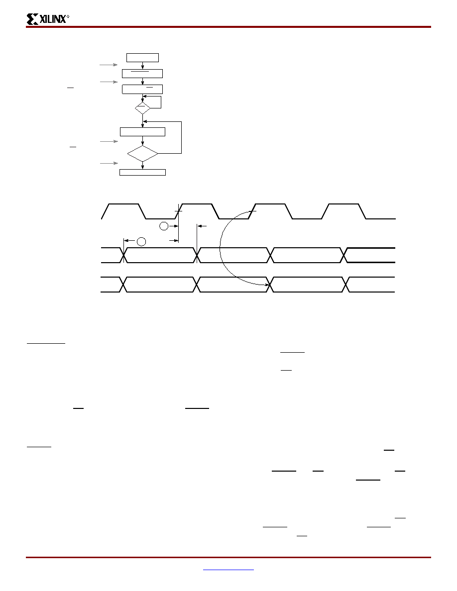
Figure 16 shows the timing of master-serial configuration.
Master-serial mode is selected by a <000> or <100> on the
mode pins (M2, M1, M0). Table 10 shows the timing infor-
mation for Figure 16.
At power-up, VCC must rise from 1.0 V to VCC Min in less
than 50 ms, otherwise delay configuration by pulling
PROGRAM Low until VCC is valid.
SelectMAP Mode
The SelectMAP mode is the fastest configuration option.
Byte-wide data is written into the FPGA with a BUSY flag
controlling the flow of data.
An external data source provides a byte stream, CCLK, a
Chip Select (CS) signal and a Write signal (WRITE). If
BUSY is asserted (High) by the FPGA, the data must be
held until BUSY goes Low.
Data can also be read using the SelectMAP mode. If
WRITE is not asserted, configuration data is read out of the
FPGA as part of a readback operation.
After configuration, the pins of the SelectMAP port can be
used as additional user I/O. Alternatively, the port can be
retained to permit high-speed 8-bit readback.
Retention of the SelectMAP port is selectable on a
design-by-design basis when the bitstream is generated. If
retention is selected, PROHIBIT constraints are required to
prevent the SelectMAP-port pins from being used as user
I/O.
Multiple Virtex-E FPGAs can be configured using the
SelectMAP mode, and be made to start-up simultaneously.
To configure multiple devices in this way, wire the individual
CCLK, Data, WRITE, and BUSY pins of all the devices in
parallel. The individual devices are loaded separately by
asserting the CS pin of each device in turn and writing the
appropriate data. See Table 11 for SelectMAP Write Timing
Characteristics.
Write
Write operations send packets of configuration data into the
FPGA. The sequence of operations for a multi-cycle write
operation is shown below. Note that a configuration packet
can be split into many such sequences. The packet does
not have to complete within one assertion of CS, illustrated
in Figure 17.
1.
Assert WRITE and CS Low. Note that when CS is
asserted on successive CCLKs, WRITE must remain
either asserted or de-asserted. Otherwise, an abort is
initiated, as described below.
2.
Drive data onto D[7:0]. Note that to avoid contention,
the data source should not be enabled while CS is Low
and WRITE is High. Similarly, while WRITE is High, no
more that one CS should be asserted.
Figure 15: Serial Configuration Flowchart
Apply Power
Set PROGRAM = High
Release INIT
If used to delay
configuration
Load a Configuration Bit
High
Low
FPGA makes a final
clearing pass and releases
INIT when finished.
FPGA starts to clear
configuration memory.
ds009_15_111799
Configuration Completed
End of
Bitstream?
Yes
No
Once per bitstream,
FPGA checks data using CRC
and pulls INIT Low on error.
If no CRC errors found,
FPGA enters start-up phase
causing DONE to go High.
INIT?
Figure 16: Master-Serial Mode Programming Switching Characteristics
Serial Data In
CCLK
(Output)
Serial DOUT
(Output)
1 TDSCK
2
TCKDS
DS022_44_071201
相关PDF资料 |
PDF描述 |
|---|---|
| SST39VF800A-70-4C-B3KE-T | IC FLASH MPF 8MBIT 70NS 48TFBGA |
| 25LC512-E/SN | IC EEPROM 512KBIT 20MHZ 8SOIC |
| 25LC512T-E/SN | IC EEPROM 512KBIT 20MHZ 8SOIC |
| SST25VF032B-66-4I-S2AF-T | IC FLASH SER 32M 66MHZ SPI 8SOIC |
| SST25VF032B-80-4I-S2AF-T | IC FLSH SER 32MB 66MHZ SPI 8SOIC |
相关代理商/技术参数 |
参数描述 |
|---|---|
| XCV300E-6FG456C0707 | 制造商:Xilinx 功能描述: |
| XCV300E-6FG456I | 功能描述:IC FPGA 1.8V I-TEMP 456-FBGA RoHS:否 类别:集成电路 (IC) >> 嵌入式 - FPGA(现场可编程门阵列) 系列:Virtex®-E 产品变化通告:Step Intro and Pkg Change 11/March/2008 标准包装:1 系列:Virtex®-5 SXT LAB/CLB数:4080 逻辑元件/单元数:52224 RAM 位总计:4866048 输入/输出数:480 门数:- 电源电压:0.95 V ~ 1.05 V 安装类型:表面贴装 工作温度:-40°C ~ 100°C 封装/外壳:1136-BBGA,FCBGA 供应商设备封装:1136-FCBGA 配用:568-5088-ND - BOARD DEMO DAC1408D750122-1796-ND - EVALUATION PLATFORM VIRTEX-5 |
| XCV300E-6HQ204C | 制造商:XILINX 制造商全称:XILINX 功能描述:Virte -E 1.8 V Field Programmable Gate Arrays |
| XCV300E-6HQ204I | 制造商:XILINX 制造商全称:XILINX 功能描述:Virte -E 1.8 V Field Programmable Gate Arrays |
| XCV300E-6HQ240C | 制造商:XILINX 制造商全称:XILINX 功能描述:Virtex-E 1.8 V Field Programmable Gate Arrays |
发布紧急采购,3分钟左右您将得到回复。