参数资料
| 型号: | XCV300E-6FG456C |
| 厂商: | Xilinx Inc |
| 文件页数: | 153/233页 |
| 文件大小: | 0K |
| 描述: | IC FPGA 1.8V C-TEMP 456-FBGA |
| 产品变化通告: | FPGA Family Discontinuation 18/Apr/2011 |
| 标准包装: | 60 |
| 系列: | Virtex®-E |
| LAB/CLB数: | 1536 |
| 逻辑元件/单元数: | 6912 |
| RAM 位总计: | 131072 |
| 输入/输出数: | 312 |
| 门数: | 411955 |
| 电源电压: | 1.71 V ~ 1.89 V |
| 安装类型: | 表面贴装 |
| 工作温度: | 0°C ~ 85°C |
| 封装/外壳: | 456-BBGA |
| 供应商设备封装: | 456-FBGA |
第1页第2页第3页第4页第5页第6页第7页第8页第9页第10页第11页第12页第13页第14页第15页第16页第17页第18页第19页第20页第21页第22页第23页第24页第25页第26页第27页第28页第29页第30页第31页第32页第33页第34页第35页第36页第37页第38页第39页第40页第41页第42页第43页第44页第45页第46页第47页第48页第49页第50页第51页第52页第53页第54页第55页第56页第57页第58页第59页第60页第61页第62页第63页第64页第65页第66页第67页第68页第69页第70页第71页第72页第73页第74页第75页第76页第77页第78页第79页第80页第81页第82页第83页第84页第85页第86页第87页第88页第89页第90页第91页第92页第93页第94页第95页第96页第97页第98页第99页第100页第101页第102页第103页第104页第105页第106页第107页第108页第109页第110页第111页第112页第113页第114页第115页第116页第117页第118页第119页第120页第121页第122页第123页第124页第125页第126页第127页第128页第129页第130页第131页第132页第133页第134页第135页第136页第137页第138页第139页第140页第141页第142页第143页第144页第145页第146页第147页第148页第149页第150页第151页第152页当前第153页第154页第155页第156页第157页第158页第159页第160页第161页第162页第163页第164页第165页第166页第167页第168页第169页第170页第171页第172页第173页第174页第175页第176页第177页第178页第179页第180页第181页第182页第183页第184页第185页第186页第187页第188页第189页第190页第191页第192页第193页第194页第195页第196页第197页第198页第199页第200页第201页第202页第203页第204页第205页第206页第207页第208页第209页第210页第211页第212页第213页第214页第215页第216页第217页第218页第219页第220页第221页第222页第223页第224页第225页第226页第227页第228页第229页第230页第231页第232页第233页
Virtex-E 1.8 V Field Programmable Gate Arrays
R
Module 2 of 4
DS022-2 (v3.0) March 21, 2014
20
Production Product Specification
— OBSOLETE — OBSOLETE — OBSOLETE — OBSOLETE —
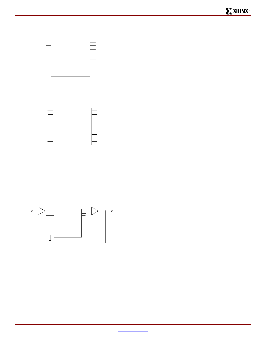
BUFGDLL Pin Descriptions
Use the BUFGDLL macro as the simplest way to provide
zero propagation delay for a high-fanout on-chip clock from
an external input. This macro uses the IBUFG, CLKDLL and
BUFG primitives to implement the most basic DLL applica-
tion as shown in Figure 24.
This symbol does not provide access to the advanced clock
domain controls or to the clock multiplication or clock divi-
sion features of the DLL. This symbol also does not provide
access to the RST, or LOCKED pins of the DLL. For access
to these features, a designer must use the library DLL prim-
itives described in the following sections.
Source Clock Input — I
The I pin provides the user source clock, the clock signal on
which the DLL operates, to the BUFGDLL. For the BUFG-
DLL macro the source clock frequency must fall in the low
frequency range as specified in the data sheet. The BUFG-
DLL requires an external signal source clock. Therefore,
only an external input port can source the signal that drives
the BUFGDLL I pin.
Clock Output — O
The clock output pin O represents a delay-compensated
version of the source clock (I) signal. This signal, sourced by
a global clock buffer BUFG symbol, takes advantage of the
dedicated global clock routing resources of the device.
The output clock has a 50-50 duty cycle unless you deacti-
vate the duty cycle correction property.
CLKDLL Primitive Pin Descriptions
The library CLKDLL primitives provide access to the com-
plete set of DLL features needed when implementing more
complex applications with the DLL.
Source Clock Input — CLKIN
The CLKIN pin provides the user source clock (the clock
signal on which the DLL operates) to the DLL. The CLKIN
frequency must fall in the ranges specified in the data sheet.
A global clock buffer (BUFG) driven from another CLKDLL,
one of the global clock input buffers (IBUFG), or an
IO_LVDS_DLL pin on the same edge of the device (top or
bottom) must source this clock signal. There are four
IO_LVDS_DLL input pins that can be used as inputs to the
DLLs. This makes a total of eight usable input pins for DLLs
in the Virtex-E family.
Feedback Clock Input — CLKFB
The DLL requires a reference or feedback signal to provide
the delay-compensated output. Connect only the CLK0 or
CLK2X DLL outputs to the feedback clock input (CLKFB)
pin to provide the necessary feedback to the DLL. The feed-
back clock input can also be provided through one of the fol-
lowing pins.
IBUFG - Global Clock Input Pad
IO_LVDS_DLL - the pin adjacent to IBUFG
If an IBUFG sources the CLKFB pin, the following special
rules apply.
1.
An external input port must source the signal that drives
the IBUFG I pin.
2.
The CLK2X output must feedback to the device if both
the CLK0 and CLK2X outputs are driving off chip
devices.
3.
That signal must directly drive only OBUFs and nothing
else.
These rules enable the software determine which DLL clock
output sources the CLKFB pin.
Reset Input — RST
When the reset pin RST activates the LOCKED signal deac-
tivates within four source clock cycles. The RST pin, active
High, must either connect to a dynamic signal or tied to
Figure 22: Standard DLL Symbol CLKDLL
Figure 23: High Frequency DLL Symbol CLKDLLHF
Figure 24: BUFGDLL Schematic
CLK0
CLK90
CLK180
CLK270
CLK2X
CLKDV
LOCKED
CLKIN
CLKFB
RST
ds022_26_121099
CLKDLL
CLK0
CLK180
CLKDV
LOCKED
CLKIN
CLKFB
RST
ds022_027_121099
CLKDLLHF
CLK0
CLK90
CLK180
CLK270
CLK2X
CLKDV
LOCKED
CLKIN
CLKFB
RST
ds022_28_121099
CLKDLL
BUFG
IBUFG
O
I
O
I
相关PDF资料 |
PDF描述 |
|---|---|
| SST39VF800A-70-4C-B3KE-T | IC FLASH MPF 8MBIT 70NS 48TFBGA |
| 25LC512-E/SN | IC EEPROM 512KBIT 20MHZ 8SOIC |
| 25LC512T-E/SN | IC EEPROM 512KBIT 20MHZ 8SOIC |
| SST25VF032B-66-4I-S2AF-T | IC FLASH SER 32M 66MHZ SPI 8SOIC |
| SST25VF032B-80-4I-S2AF-T | IC FLSH SER 32MB 66MHZ SPI 8SOIC |
相关代理商/技术参数 |
参数描述 |
|---|---|
| XCV300E-6FG456C0707 | 制造商:Xilinx 功能描述: |
| XCV300E-6FG456I | 功能描述:IC FPGA 1.8V I-TEMP 456-FBGA RoHS:否 类别:集成电路 (IC) >> 嵌入式 - FPGA(现场可编程门阵列) 系列:Virtex®-E 产品变化通告:Step Intro and Pkg Change 11/March/2008 标准包装:1 系列:Virtex®-5 SXT LAB/CLB数:4080 逻辑元件/单元数:52224 RAM 位总计:4866048 输入/输出数:480 门数:- 电源电压:0.95 V ~ 1.05 V 安装类型:表面贴装 工作温度:-40°C ~ 100°C 封装/外壳:1136-BBGA,FCBGA 供应商设备封装:1136-FCBGA 配用:568-5088-ND - BOARD DEMO DAC1408D750122-1796-ND - EVALUATION PLATFORM VIRTEX-5 |
| XCV300E-6HQ204C | 制造商:XILINX 制造商全称:XILINX 功能描述:Virte -E 1.8 V Field Programmable Gate Arrays |
| XCV300E-6HQ204I | 制造商:XILINX 制造商全称:XILINX 功能描述:Virte -E 1.8 V Field Programmable Gate Arrays |
| XCV300E-6HQ240C | 制造商:XILINX 制造商全称:XILINX 功能描述:Virtex-E 1.8 V Field Programmable Gate Arrays |
发布紧急采购,3分钟左右您将得到回复。