参数资料
| 型号: | XCV300E-6FG456C |
| 厂商: | Xilinx Inc |
| 文件页数: | 220/233页 |
| 文件大小: | 0K |
| 描述: | IC FPGA 1.8V C-TEMP 456-FBGA |
| 产品变化通告: | FPGA Family Discontinuation 18/Apr/2011 |
| 标准包装: | 60 |
| 系列: | Virtex®-E |
| LAB/CLB数: | 1536 |
| 逻辑元件/单元数: | 6912 |
| RAM 位总计: | 131072 |
| 输入/输出数: | 312 |
| 门数: | 411955 |
| 电源电压: | 1.71 V ~ 1.89 V |
| 安装类型: | 表面贴装 |
| 工作温度: | 0°C ~ 85°C |
| 封装/外壳: | 456-BBGA |
| 供应商设备封装: | 456-FBGA |
第1页第2页第3页第4页第5页第6页第7页第8页第9页第10页第11页第12页第13页第14页第15页第16页第17页第18页第19页第20页第21页第22页第23页第24页第25页第26页第27页第28页第29页第30页第31页第32页第33页第34页第35页第36页第37页第38页第39页第40页第41页第42页第43页第44页第45页第46页第47页第48页第49页第50页第51页第52页第53页第54页第55页第56页第57页第58页第59页第60页第61页第62页第63页第64页第65页第66页第67页第68页第69页第70页第71页第72页第73页第74页第75页第76页第77页第78页第79页第80页第81页第82页第83页第84页第85页第86页第87页第88页第89页第90页第91页第92页第93页第94页第95页第96页第97页第98页第99页第100页第101页第102页第103页第104页第105页第106页第107页第108页第109页第110页第111页第112页第113页第114页第115页第116页第117页第118页第119页第120页第121页第122页第123页第124页第125页第126页第127页第128页第129页第130页第131页第132页第133页第134页第135页第136页第137页第138页第139页第140页第141页第142页第143页第144页第145页第146页第147页第148页第149页第150页第151页第152页第153页第154页第155页第156页第157页第158页第159页第160页第161页第162页第163页第164页第165页第166页第167页第168页第169页第170页第171页第172页第173页第174页第175页第176页第177页第178页第179页第180页第181页第182页第183页第184页第185页第186页第187页第188页第189页第190页第191页第192页第193页第194页第195页第196页第197页第198页第199页第200页第201页第202页第203页第204页第205页第206页第207页第208页第209页第210页第211页第212页第213页第214页第215页第216页第217页第218页第219页当前第220页第221页第222页第223页第224页第225页第226页第227页第228页第229页第230页第231页第232页第233页
2000-2014 Xilinx, Inc. All rights reserved. All Xilinx trademarks, registered trademarks, patents, and disclaimers are as listed at http://www.xilinx.com/legal.htm.
All other trademarks and registered trademarks are the property of their respective owners. All specifications are subject to change without notice.
DS022-4 (v3.0) March 21, 2014
Module 4 of 4
Production Product Specification
1
— OBSOLETE — OBSOLETE — OBSOLETE — OBSOLETE —
Virtex-E Pin Definitions
0
Virtex-E 1.8 V
Field Programmable Gate Arrays
DS022-4 (v3.0) March 21, 2014
00
Production Product Specification
R
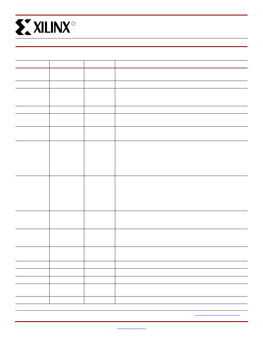
Pin Name
Dedicated Pin
Direction
Description
GCK0, GCK1,
GCK2, GCK3
Yes
Input
Clock input pins that connect to Global Clock Buffers.
M0, M1, M2
Yes
Input
Mode pins are used to specify the configuration mode.
CCLK
Yes
Input or
Output
The configuration Clock I/O pin: it is an input for SelectMAP and
slave-serial modes, and output in master-serial mode. After
configuration, it is input only, logic level = Don’t Care.
PROGRAM
Yes
Input
Initiates a configuration sequence when asserted Low.
DONE
Yes
Bidirectional
Indicates that configuration loading is complete, and that the start-up
sequence is in progress. The output can be open drain.
INIT
No
Bidirectional
(Open-drain)
When Low, indicates that the configuration memory is being cleared.
The pin becomes a user I/O after configuration.
BUSY/DOUT
No
Output
In SelectMAP mode, BUSY controls the rate at which configuration
data is loaded. The pin becomes a user I/O after configuration unless
the SelectMAP port is retained.
In bit-serial modes, DOUT provides preamble and configuration data
to downstream devices in a daisy-chain. The pin becomes a user I/O
after configuration.
D0/DIN,
D1, D2,
D3, D4,
D5, D6,
D7
No
Input or
Output
In SelectMAP mode, D0-7 are configuration data pins. These pins
become user I/Os after configuration unless the SelectMAP port is
retained.
In bit-serial modes, DIN is the single data input. This pin becomes a
user I/O after configuration.
WRITE
No
Input
In SelectMAP mode, the active-low Write Enable signal. The pin
becomes a user I/O after configuration unless the SelectMAP port is
retained.
CS
No
Input
In SelectMAP mode, the active-low Chip Select signal. The pin
becomes a user I/O after configuration unless the SelectMAP port is
retained.
TDI, TDO,
TMS, TCK
Yes
Mixed
Boundary-scan Test-Access-Port pins, as defined in IEEE1149.1.
DXN, DXP
Yes
N/A
Temperature-sensing diode pins. (Anode: DXP, cathode: DXN)
VCCINT
Yes
Input
Power-supply pins for the internal core logic.
VCCO
Yes
Input
Power-supply pins for the output drivers (subject to banking rules)
VREF
No
Input
Input threshold voltage pins. Become user I/Os when an external
threshold voltage is not needed (subject to banking rules).
GND
Yes
Input
Ground
相关PDF资料 |
PDF描述 |
|---|---|
| SST39VF800A-70-4C-B3KE-T | IC FLASH MPF 8MBIT 70NS 48TFBGA |
| 25LC512-E/SN | IC EEPROM 512KBIT 20MHZ 8SOIC |
| 25LC512T-E/SN | IC EEPROM 512KBIT 20MHZ 8SOIC |
| SST25VF032B-66-4I-S2AF-T | IC FLASH SER 32M 66MHZ SPI 8SOIC |
| SST25VF032B-80-4I-S2AF-T | IC FLSH SER 32MB 66MHZ SPI 8SOIC |
相关代理商/技术参数 |
参数描述 |
|---|---|
| XCV300E-6FG456C0707 | 制造商:Xilinx 功能描述: |
| XCV300E-6FG456I | 功能描述:IC FPGA 1.8V I-TEMP 456-FBGA RoHS:否 类别:集成电路 (IC) >> 嵌入式 - FPGA(现场可编程门阵列) 系列:Virtex®-E 产品变化通告:Step Intro and Pkg Change 11/March/2008 标准包装:1 系列:Virtex®-5 SXT LAB/CLB数:4080 逻辑元件/单元数:52224 RAM 位总计:4866048 输入/输出数:480 门数:- 电源电压:0.95 V ~ 1.05 V 安装类型:表面贴装 工作温度:-40°C ~ 100°C 封装/外壳:1136-BBGA,FCBGA 供应商设备封装:1136-FCBGA 配用:568-5088-ND - BOARD DEMO DAC1408D750122-1796-ND - EVALUATION PLATFORM VIRTEX-5 |
| XCV300E-6HQ204C | 制造商:XILINX 制造商全称:XILINX 功能描述:Virte -E 1.8 V Field Programmable Gate Arrays |
| XCV300E-6HQ204I | 制造商:XILINX 制造商全称:XILINX 功能描述:Virte -E 1.8 V Field Programmable Gate Arrays |
| XCV300E-6HQ240C | 制造商:XILINX 制造商全称:XILINX 功能描述:Virtex-E 1.8 V Field Programmable Gate Arrays |
发布紧急采购,3分钟左右您将得到回复。