参数资料
| 型号: | XCV300E-6FG456C |
| 厂商: | Xilinx Inc |
| 文件页数: | 155/233页 |
| 文件大小: | 0K |
| 描述: | IC FPGA 1.8V C-TEMP 456-FBGA |
| 产品变化通告: | FPGA Family Discontinuation 18/Apr/2011 |
| 标准包装: | 60 |
| 系列: | Virtex®-E |
| LAB/CLB数: | 1536 |
| 逻辑元件/单元数: | 6912 |
| RAM 位总计: | 131072 |
| 输入/输出数: | 312 |
| 门数: | 411955 |
| 电源电压: | 1.71 V ~ 1.89 V |
| 安装类型: | 表面贴装 |
| 工作温度: | 0°C ~ 85°C |
| 封装/外壳: | 456-BBGA |
| 供应商设备封装: | 456-FBGA |
第1页第2页第3页第4页第5页第6页第7页第8页第9页第10页第11页第12页第13页第14页第15页第16页第17页第18页第19页第20页第21页第22页第23页第24页第25页第26页第27页第28页第29页第30页第31页第32页第33页第34页第35页第36页第37页第38页第39页第40页第41页第42页第43页第44页第45页第46页第47页第48页第49页第50页第51页第52页第53页第54页第55页第56页第57页第58页第59页第60页第61页第62页第63页第64页第65页第66页第67页第68页第69页第70页第71页第72页第73页第74页第75页第76页第77页第78页第79页第80页第81页第82页第83页第84页第85页第86页第87页第88页第89页第90页第91页第92页第93页第94页第95页第96页第97页第98页第99页第100页第101页第102页第103页第104页第105页第106页第107页第108页第109页第110页第111页第112页第113页第114页第115页第116页第117页第118页第119页第120页第121页第122页第123页第124页第125页第126页第127页第128页第129页第130页第131页第132页第133页第134页第135页第136页第137页第138页第139页第140页第141页第142页第143页第144页第145页第146页第147页第148页第149页第150页第151页第152页第153页第154页当前第155页第156页第157页第158页第159页第160页第161页第162页第163页第164页第165页第166页第167页第168页第169页第170页第171页第172页第173页第174页第175页第176页第177页第178页第179页第180页第181页第182页第183页第184页第185页第186页第187页第188页第189页第190页第191页第192页第193页第194页第195页第196页第197页第198页第199页第200页第201页第202页第203页第204页第205页第206页第207页第208页第209页第210页第211页第212页第213页第214页第215页第216页第217页第218页第219页第220页第221页第222页第223页第224页第225页第226页第227页第228页第229页第230页第231页第232页第233页
Virtex-E 1.8 V Field Programmable Gate Arrays
R
Module 2 of 4
DS022-2 (v3.0) March 21, 2014
22
Production Product Specification
— OBSOLETE — OBSOLETE — OBSOLETE — OBSOLETE —
DLL Properties
Properties provide access to some of the Virtex-E series
DLL features, (for example, clock division and duty cycle
correction).
Duty Cycle Correction Property
The 1x clock outputs, CLK0, CLK90, CLK180, and CLK270,
use the duty-cycle corrected default, exhibiting a 50/50 duty
cycle. The DUTY_CYCLE_CORRECTION property (by
default TRUE) controls this feature. To deactivate the DLL
duty-cycle correction for the 1x clock outputs, attach the
DUTY_CYCLE_CORRECTION=FALSE property to the
DLL symbol.
Clock Divide Property
The CLKDV_DIVIDE property specifies how the signal on
the CLKDV pin is frequency divided with respect to the
CLK0 pin. The values allowed for this property are 1.5, 2,
2.5, 3, 4, 5, 8, or 16; the default value is 2.
Startup Delay Property
This property, STARTUP_WAIT, takes on a value of TRUE
or FALSE (the default value). When TRUE the device con-
figuration DONE signal waits until the DLL locks before
going to High.
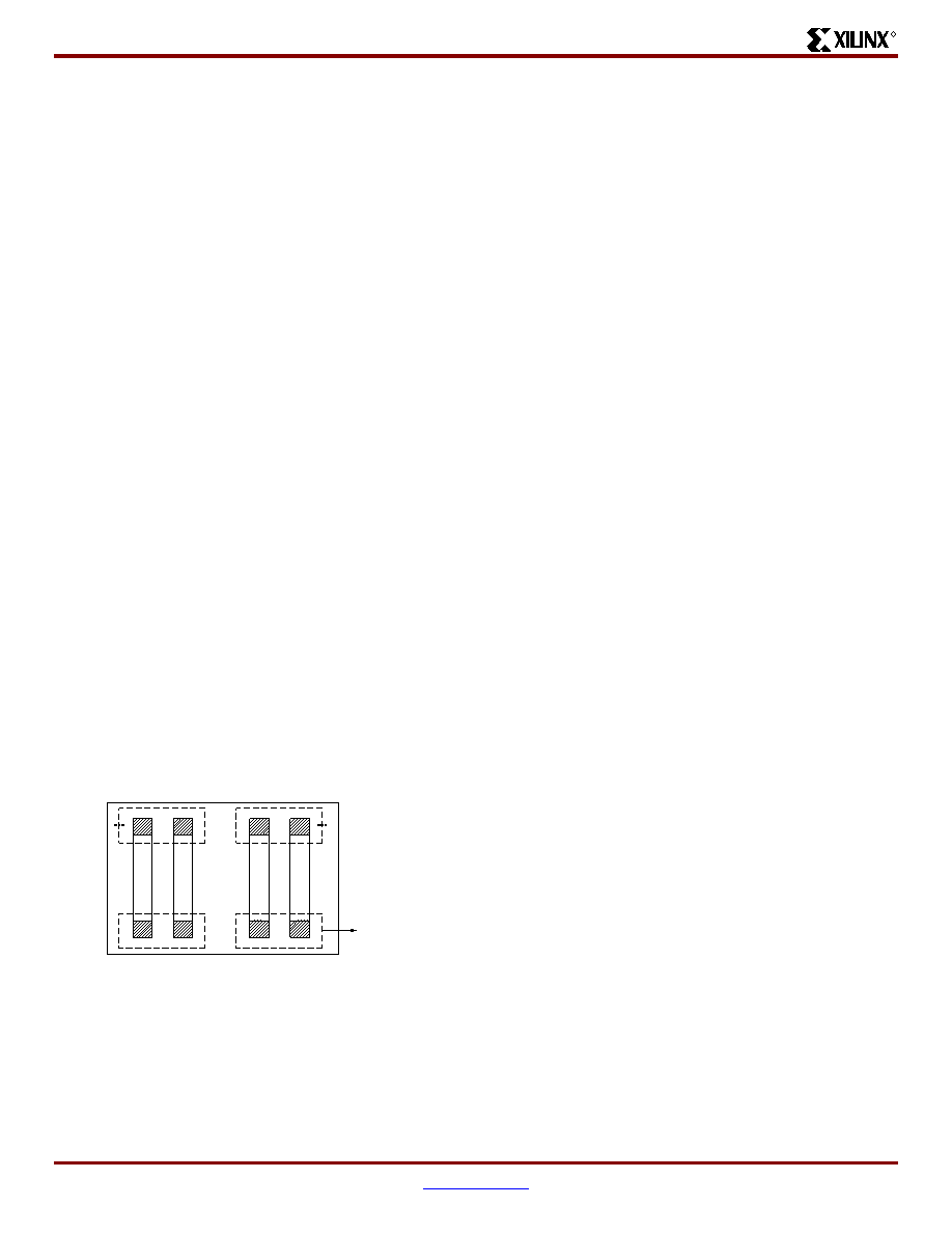
Virtex-E DLL Location Constraints
As shown in Figure 26, there are four additional DLLs in the
Virtex-E devices, for a total of eight per Virtex-E device.
These DLLs are located in silicon, at the top and bottom of
the two innermost block SelectRAM columns. The location
constraint LOC, attached to the DLL symbol with the identi-
fier DLL0S, DLL0P, DLL1S, DLL1P, DLL2S, DLL2P, DLL3S,
or DLL3P, controls the DLL location.
The LOC property uses the following form:
LOC = DLL0P
Design Factors
Use the following design considerations to avoid pitfalls and
improve success designing with Xilinx devices.
Input Clock
The output clock signal of a DLL, essentially a delayed ver-
sion of the input clock signal, reflects any instability on the
input clock in the output waveform. For this reason the qual-
ity of the DLL input clock relates directly to the quality of the
output clock waveforms generated by the DLL. The DLL
input clock requirements are specified in the data sheet.
In most systems a crystal oscillator generates the system
clock. The DLL can be used with any commercially available
quartz crystal oscillator. For example, most crystal oscilla-
tors produce an output waveform with a frequency tolerance
of 100 PPM, meaning 0.01 percent change in the clock
period. The DLL operates reliably on an input waveform with
a frequency drift of up to 1 ns — orders of magnitude in
excess of that needed to support any crystal oscillator in the
industry. However, the cycle-to-cycle jitter must be kept to
less than 300 ps in the low frequencies and 150 ps for the
high frequencies.
Input Clock Changes
Changing the period of the input clock beyond the maximum
drift amount requires a manual reset of the CLKDLL. Failure
to reset the DLL produces an unreliable lock signal and out-
put clock.
It is possible to stop the input clock with little impact to the
DLL. Stopping the clock should be limited to less than
100
μs to keep device cooling to a minimum. The clock
should be stopped during a Low phase, and when restored
the full High period should be seen. During this time,
LOCKED stays High and remains High when the clock is
restored.
When the clock is stopped, one to four more clocks are still
observed as the delay line is flushed. When the clock is
restarted, the output clocks are not observed for one to four
clocks as the delay line is filled. The most common case is
two or three clocks.
In a similar manner, a phase shift of the input clock is also
possible. The phase shift propagates to the output one to
four clocks after the original shift, with no disruption to the
CLKDLL control.
Output Clocks
As mentioned earlier in the DLL pin descriptions, some
restrictions apply regarding the connectivity of the output
pins. The DLL clock outputs can drive an OBUF, a global
clock buffer BUFG, or they can route directly to destination
clock pins. The only BUFGs that the DLL clock outputs can
drive are the two on the same edge of the device (top or bot-
tom). In addition, the CLK2X output of the secondary DLL
can connect directly to the CLKIN of the primary DLL in the
same quadrant.
Do not use the DLL output clock signals until after activation
of the LOCKED signal. Prior to the activation of the
LOCKED signal, the DLL output clocks are not valid and
can exhibit glitches, spikes, or other spurious movement.
Figure 26: Virtex Series DLLs
x132_14_100799
B
R
A
M
DLL-3P
DLL-1P
DLL-3S
DLL-1S
DLL-2S
DLL-0S
DLL-2P
DLL-0P
Bottom Right
Half Edge
B
R
A
M
B
R
A
M
B
R
A
M
相关PDF资料 |
PDF描述 |
|---|---|
| SST39VF800A-70-4C-B3KE-T | IC FLASH MPF 8MBIT 70NS 48TFBGA |
| 25LC512-E/SN | IC EEPROM 512KBIT 20MHZ 8SOIC |
| 25LC512T-E/SN | IC EEPROM 512KBIT 20MHZ 8SOIC |
| SST25VF032B-66-4I-S2AF-T | IC FLASH SER 32M 66MHZ SPI 8SOIC |
| SST25VF032B-80-4I-S2AF-T | IC FLSH SER 32MB 66MHZ SPI 8SOIC |
相关代理商/技术参数 |
参数描述 |
|---|---|
| XCV300E-6FG456C0707 | 制造商:Xilinx 功能描述: |
| XCV300E-6FG456I | 功能描述:IC FPGA 1.8V I-TEMP 456-FBGA RoHS:否 类别:集成电路 (IC) >> 嵌入式 - FPGA(现场可编程门阵列) 系列:Virtex®-E 产品变化通告:Step Intro and Pkg Change 11/March/2008 标准包装:1 系列:Virtex®-5 SXT LAB/CLB数:4080 逻辑元件/单元数:52224 RAM 位总计:4866048 输入/输出数:480 门数:- 电源电压:0.95 V ~ 1.05 V 安装类型:表面贴装 工作温度:-40°C ~ 100°C 封装/外壳:1136-BBGA,FCBGA 供应商设备封装:1136-FCBGA 配用:568-5088-ND - BOARD DEMO DAC1408D750122-1796-ND - EVALUATION PLATFORM VIRTEX-5 |
| XCV300E-6HQ204C | 制造商:XILINX 制造商全称:XILINX 功能描述:Virte -E 1.8 V Field Programmable Gate Arrays |
| XCV300E-6HQ204I | 制造商:XILINX 制造商全称:XILINX 功能描述:Virte -E 1.8 V Field Programmable Gate Arrays |
| XCV300E-6HQ240C | 制造商:XILINX 制造商全称:XILINX 功能描述:Virtex-E 1.8 V Field Programmable Gate Arrays |
发布紧急采购,3分钟左右您将得到回复。